From LBL: “Copper is Key in Burning Fat”

Berkeley Logo

Berkeley Lab

1
Chris Chang and UC Berkeley graduate student Sumin Lee carry out experiments to find proteins that bind to copper and potentially influence the storage and burning of fat. (Credit: Peg Skorpinski/UC Berkeley)

Long prized as a malleable, conductive metal used in cookware, electronics, jewelry and plumbing, copper has been gaining increasing attention over the past decade for its role in certain biological functions. It has been known that copper is needed to form red blood cells, absorb iron, develop connective tissue and support the immune system.

The new findings, to appear in the July print issue of Nature Chemical Biology but published online today, establishes for the first time copper’s role in fat metabolism.

The team of researchers was led by Chris Chang, a faculty scientist at Berkeley Lab’s Chemical Sciences Division, a UC Berkeley professor of chemistry and a Howard Hughes Medical Institute investigator. Co-lead authors of the study are Lakshmi Krishnamoorthy and Joseph Cotruvo Jr, both UC Berkeley postdoctoral researchers in chemistry with affiliations at Berkeley Lab.

“We find that copper is essential for breaking down fat cells so that they can be used for energy,” said Chang. “It acts as a regulator. The more copper there is, the more the fat is broken down. We think it would be worthwhile to study whether a deficiency in this nutrient could be linked to obesity and obesity-related diseases.”

Dietary copper

Chang said that copper could potentially play a role in restoring a natural way to burn fat. The nutrient is plentiful in foods such as oysters and other shellfish, leafy greens, mushrooms, seeds, nuts and beans.

According to the Food and Nutrition Board of the Institute of Medicine, an adult’s estimated average dietary requirement for copper is about 700 micrograms per day. The Food and Nutrition Board also found that only 25 percent of the U.S. population gets enough copper daily.

“Copper is not something the body can make, so we need to get it through our diet,” said Chang. “The typical American diet, however, doesn’t include many green leafy vegetables. Asian diets, for example, have more foods rich in copper.”

But Chang cautions against ingesting copper supplements as a result of these study results. Too much copper can lead to imbalances with other essential minerals, including zinc.

Copper as a ‘brake on a brake’

The researchers made the copper-fat link using mice with a genetic mutation that causes the accumulation of copper in the liver. Notably, these mice have larger than average deposits of fat compared with normal mice.

2
A fluorescent probe creates a heat map of copper in white fat cells. Higher levels of copper are shown in yellow and red. The left panel shows normal levels of copper from fat cells of control mice, and the right panel shows cells deficient in copper. (Credit: Lakshmi Krishnamoorthy and Joseph Cotruvo Jr./UC Berkeley)

The inherited condition, known as Wilson’s disease, also occurs in humans and is potentially fatal if left untreated.

Analysis of the mice with Wilson’s disease revealed that the abnormal buildup of copper was accompanied by lower than normal lipid levels in the liver compared with control groups of mice. The researchers also found that the white adipose tissue, or white fat, of the mice with Wilson’s disease had lower levels of copper compared with the control mice and correspondingly higher levels of fat deposits.

They then treated the Wilson’s disease mice with isoproterenol, a beta agonist known to induce lipolysis, the breakdown of fat into fatty acids, through the cyclic adenosine monophosphate (cAMP) signaling pathway. They noted that the mice with Wilson’s disease exhibited less fat-breakdown activity compared with control mice.

The results prompted the researchers to conduct cell culture analyses to clarify the mechanism by which copper influences lipolysis. The researchers used inductively coupled plasma mass spectroscopy (ICP-MS) equipment at Berkeley Lab to measure levels of copper in fat tissue.

They found that copper binds to phosphodiesterase 3, or PDE3, an enzyme that binds to cAMP, halting cAMP’s ability to facilitate the breakdown of fat.

“When copper binds phosphodiesterase, it’s like a brake on a brake,” said Chang. “That’s why copper has a positive correlation with lipolysis.”

Hints from cows and copper

The connection between copper and fat metabolism is not altogether surprising. The researchers actually found hints of the link in the field of animal husbandry.

“It had been noted in cattle that levels of copper in the feed would affect how fatty the meat was,” said Chang. “This effect on fat deposits in animals was in the agricultural literature, but it hadn’t been clear what the biochemical mechanisms were linking copper and fat.”

The new work builds upon prior research from Chang’s lab on the roles of copper and other metals in neuroscience. In support of President Barack Obama’s BRAIN Initiative, Berkeley Lab provided Chang seed funding in 2013 through the Laboratory Directed Research and Development program. Chang’s work continued through the BRAIN Tri-Institutional Partnership, an alliance with Berkeley Lab, UC Berkeley and UC San Francisco.

Of the copper in human bodies, there are particularly high concentrations found in the brain. Recent studies, including those led by Chang, have found that copper helps brain cells communicate with each other by acting as a brake when it is time for neural signals to stop.

While Chang’s initial focus was on the role of copper in neural communications, he branched out to investigations of metals in fat metabolism and other biological pathways. This latest work was primarily funded by the National Institutes of Health.

Previous stories on Chris Chang’s research on copper include:

Copper on the Brain at Rest
Of Metal Heads and Imaging

A profile of Chris Chang is online through the UC Berkeley Office of the Vice Chancellor for Research.

See the full article here .

Please help promote STEM in your local schools.

STEM Icon

Stem Education Coalition

A U.S. Department of Energy National Laboratory Operated by the University of California

University of California Seal

DOE Seal

From FNAL: “Upgraded PIP-II RFQ successfully takes first beam”

FNAL II photo

FNAL Art Image
FNAL Art Image by Angela Gonzales

Fermilab is an enduring source of strength for the US contribution to scientific research world wide.

May 25, 2016
Rashmi Shivni

1
This photo of the RFQ for the Fermilab PIP-II accelerator was taken during the assembly phase at Lawrence Berkeley National Laboratory. Photo courtesy of Andrew Lambert, Berkeley Lab

In March, the Fermilab Accelerator Division successfully sent beam through a newly commissioned linear accelerator. The brand new radio-frequency quadrupole (RFQ) linac, designed and built by a team of engineers and physicists at Lawrence Berkeley National Laboratory, will be the start for a proposed upgrade to Fermilab’s 800-MeV superconducting linear accelerator.

“The RFQ is one of the biggest challenges faced by our group,” said Derun Li, lead scientist on the RFQ development team and deputy head of the Center for Beam Physics at Berkeley Lab. “And seeing it take nearly 100 percent of the source beam on its first try is great!”

The new, front-end accelerator is one of several upgrade projects conducted under PIP-II, a plan to overhaul the Fermilab accelerator complex to produce high-intensity proton beams for the lab’s multiple experiments. PIP-II is supported by the DOE Office of Science.

Currently located at the Cryomodule Test Facility, approximately 1.5 miles northeast of Wilson Hall, the RFQ took first beam – 100-microsecond pulses at 10 hertz – during its first testing phase. Since its first run in March, the team has been working on various commissioning activities, including running the pulsed beam through the RFQ and its transport lines. These activities are expected to continue until June.

The goal of these tests is to provide intense, focused beams to the entire accelerator complex. The lab’s current RFQ, which sits at the beginning of the laboratory’s accelerator chain, accelerates a negative hydrogen ion beam to 0.75 million electronvolts, or MeV. The new RFQ, which is longer, accelerates a beam to 2.1 MeV, nearly three times the energy. Transported beam current, and therefore power, is the key improvement with the new RFQ. The current RFQ delivers 54-watt beam power; the new RFQ delivers beam at 21 kilowatts – an increase by a factor of nearly 400.

RFQs are widely used for accelerating low-energy ion beams, and the energy of the beams they produce typically caps off at about 5 MeV, said Paul Derwent, PIP-II Department head. These low energy protons will then undergo further acceleration by other components of Fermi’s accelerator complex, some to 8 GeV and others to 120 GeV.

The new RFQ is 4.5 meters long and made of four parallel copper vanes, as opposed to four rods used on the current RFQ. As viewed from one end, the vanes form a symmetrical cross. At the center of the cross is a tiny aperture, or tunnel through which the beam travels.


The RFQ is undergoing tests at the Cryomodule Test Facility at Fermilab. Photo: Reidar Hahn

If you were to remove one vane and peer inside the RFQ from the side, you would see an intricate pattern of peaks and valleys, similar to a waveform, along the inner edge of each vane. Like puzzle pieces, the vanes fit together to form the small tunnel with the rippling walls of that inner waveform shape. The farther down the tunnel you go, and therefore the higher the beam energy, the longer the spacing of the peaks and valleys. This means that the time the beam needs to go from peak to valley and back remains constant, necessary for proper acceleration.

Jim Steimel, the electrical engineering coordinator for PIP-II and a Fermilab liaison for Berkeley’s RFQ development team, said this shape is a special trait in RFQs; one that creates an electromagnetic quadrupole field that focuses low-velocity particles.

“As the beam travels through the RFQ tunnel, longitudinal electrical fields generated by the vane peaks and valleys accelerate particle energy,” Steimel said. “This helps focus the beam and keeps the particles accelerating.”

The Berkeley team successfully designed the accelerator to bring beams to a higher intensity than Fermilab’s previous RFQ technology could achieve – energy that matches PIP-II’s front-end requirements.

“Our challenge was to come up with a design that uses minimum radio-frequency power and delivers the required beam quality and intensity, and to engineer a mechanical design that can withstand continuous operation at high average power,” Li said.

Li’s team took into account potential problems that may occur at a power of 100 kilowatts or more, which was needed to maintain the electromagnetic quadrupole field inside the RFQ.

For example, at higher powers temperatures can rapidly increase, causing thermal stress on the RFQ components. Large water flow rates and durable materials are needed to withstand heat and prevent deformations, which is a significant mechanical engineering feat.

“The Berkeley team is proud to have been a key contributor to the first phase of the PIP-II upgrade,” said Wim Leemans, director of Berkeley Lab’s Accelerator Technology and Applied Physics Division. “Berkeley physicists and engineers have been building RFQs for a number of users and purposes for 30 years, and this is a great example of getting the most leverage out of the agency investment.”

Now that the Berkeley and Fermilab teams demonstrated that the RFQ can generate intense beams in pulses, the next step will be to create a continuous high-intensity beam for PIP-II. The team expects to achieve a continuous beam in the summer.

“Fermilab and Berkeley have a long history of collaboration,” Derwent said. “This was just another one where it has worked very well, and their expertise helped us achieve one of our goals.”

See the full article here .

Please help promote STEM in your local schools.

STEM Icon

Stem Education Coalition

Fermilab Campus

Fermi National Accelerator Laboratory (Fermilab), located just outside Batavia, Illinois, near Chicago, is a US Department of Energy national laboratory specializing in high-energy particle physics. Fermilab is America’s premier laboratory for particle physics and accelerator research, funded by the U.S. Department of Energy. Thousands of scientists from universities and laboratories around the world
collaborate at Fermilab on experiments at the frontiers of discovery.

From LBL: “Hunting for Dark Matter’s ‘Hidden Valley’ ” Women in Science

Berkeley Logo

Berkeley Lab

May 24, 2016
Glenn Roberts Jr.
510-486-5582
geroberts@lbl.gov

1
Kathryn Zurek (Credit: Roy Kaltschmidt/Berkeley Lab)

Kathryn Zurek realized a decade ago that we may be searching in the wrong places for clues to one of the universe’s greatest unsolved mysteries: dark matter. Despite making up an estimated 85 percent of the total mass of the universe, we haven’t yet figured out what it’s made of.

Now, Zurek, a theoretical physicist at the Department of Energy’s Lawrence Berkeley National Laboratory (Berkeley Lab), says thanks to extraordinary improvements in experimental sensitivity, “We increasingly know where not to look.” In 2006, during grad school, Zurek began to explore the concept of a new “Hidden Valley” model for physics that could hold all of the answers to dark matter.

“I noticed that from a model-builder’s point of view that dark matter was extraordinarily undeveloped,” she said. It seemed as though scientists were figuratively hunting in the dark for answers. “People were focused on models of just two classes of dark matter candidates, rather than a much broader array of possibilities.”

Physicist and author Alan Lightman has described dark matter as an “invisible elephant in the room”—you know it’s there because of the dent it’s making in the floorboards but you can’t see or touch it. Likewise, physicists can infer that dark matter exists in huge supply compared to normal matter because of its gravitational effects, which far exceed those expected from the matter we can see in space.

Since physicist Fritz Zwicky in 1933 measured this major discrepancy in the gravitational mass of a galaxy cluster, that he concluded was due to dark matter, the search for what dark matter is really made of has taken many forms: from deep-underground detectors to space- and ground-based observatories, balloon-borne missions and powerful particle accelerator experiments.

While there have been some candidate signals and hints, and numerous experiments have narrowed the range of energies and masses at which we are now looking for dark matter particles, the scientific community hasn’t yet embraced a dark matter discovery.

3 Knowns and 3 Unknowns about Dark Matter

What’s known
1. We can observe its effects.
2

2. It is abundant.
3
It makes up about 85 percent of the total mass of the universe, and about 27 percent of the universe’s total mass and energy.

3. We know more about what dark matter is not.

Increasingly sensitive detectors are lowering the possible rate at which dark mark matter particles can interact with normal matter.
4
This chart shows the sensitivity limits (solid-line curves) of various experiments searching for signs of theoretical dark matter particles known as WIMPs (weakly interacting massive particles). The shaded closed contours show hints of WIMP signals. The thin dashed and dotted curves show projections for future U.S.-led dark matter direct-detection experiments expected in the next decade, and the thick dashed curve (orange) shows a so-called “neutrino floor” where neutrino-related signals can obscure the direct detection of dark matter particles. (Credit: Snowmass report, 2013.)

What’s unknown

1. Is it made up of one particle or many particles?
6
(Credit: Pixabay/CreativeMagic)

Could dark matter be composed of an entire family of particles, such as a theorized “hidden valley” or “dark sector?”
2. Are there “dark forces” acting on dark matter?

Are there forces beyond gravity and other known forces that act on dark matter but not on ordinary matter, and can dark matter interact with itself?
7
This image from the NASA/ESA Hubble Space Telescope shows the galaxy cluster Abell 3827. The blue structures surrounding the central galaxies are views of a more distant galaxy behind the cluster that has been distorted by an effect known as gravitational lensing. Observations of the central four merging galaxies in this image have provided hints that the dark matter around one of the galaxies is not moving with the galaxy itself, possibly indicating the occurrence of an unknown type of dark matter interaction. (Credit: ESO)

3. Is there dark antimatter?
8
A computerized visualization showing the possible large-scale structure of dark matter in the universe. (Credit: Amit Chourasia and Steve Cutchin/NPACI Visualization Services; Enzo)

In 2006, as a graduate student at the University of Washington, Zurek and collaborator Matthew J. Strassler, a faculty member, published a paper*, “Echoes of a Hidden Valley at Hadron Colliders,” that considered the possibility of new physics such as the existence of a new group of light (low-mass), long-lived particles that could possibly be revealed at CERN’s Large Hadron Collider, the machine that would later enable the Nobel Prize-winning discovery of the Higgs boson in 2012.

CERN/LHC Map
CERN LHC Grand Tunnel
CERN LHC particles
LHC at CERN

Some of the scientifically popular hypothetical particle candidates for dark matter are WIMPs (weakly interacting massive particles) and axions (very-low-mass particles). But the possibility of a rich and overlooked mix of light particles was compelling for Zurek, who began to construct models to test out the theory.

“If you had a low-mass hidden sector, you could ‘stuff’ all kinds of things inside of it,” she said. “That really set me up to start thinking about complex dark sectors, which I did as a postdoc.”

Looking back to 2008, Zurek said she felt like someone carrying around a sandwich board proclaiming that dark matter could be a stranger, manifold thing than most had imagined. “I was like that little guy with the sign.”

By coincidence, the so-called “PAMELA anomaly” was revealed that same year; data from the PAMELA space mission in 2008 had found an unexpected excess of positrons, the antimatter counterpart to electrons, at certain energies. This measurement excited physicists as a possible particle signature from the decay of dark matter, and the excess defied standard dark matter theories and opened the door to new ones.

Now that the concept of “hidden valleys” or “dark sectors” with myriad particles making up dark matter is gaining steam among scientists—Zurek spoke in late April at a three-day “Workshop on Dark Sectors”—she said she feels gratified to have worked on some of the early theoretical models.

“It’s great in one sense because these ideas really got traction,” Zurek said. “The fact that there were these experimental anomalies, that was sort of a coincidence. As a second- or third-year postdoc, this was like ‘my program’—this was the thing I was pushing. It suddenly got very popular.”

On an afternoon in late April, Zurek and her student Katelin Schutz sat together waiting to press the button to submit a new paper on a proposal to tease out a signal for light dark matter particles using an exotic, supercooled liquid known as superfluid helium. In the paper, they explain how this form of helium can probe for signals of “super light dark matter,” with an energy signature well below the reach of today’s experiments.

They are also working with Dan McKinsey, a Berkeley Lab scientist and UC Berkeley physics professor who is a superfluid helium expert, on possible designs for an experiment.

Most popular theories of WIMPs suggest a mass around 100 times the mass of a proton, a particle found at an atom’s core, for example, but a superfluid helium detector could be sensitive to masses many orders of magnitude smaller, she said.

Are we any closer to finding dark matter?

Zurek said she is surprised we haven’t yet made a discovery, but she is encouraged by the increasing sensitivity of experiments, and she said Berkeley Lab has particular expertise in high-precision detectors that will hopefully ensure its role in future experiments.

“There is a cross-fertilization from different fields of physics that has really blossomed in the last several years,” Zurek also said. She joined Berkeley Lab in 2014 after serving as an associate professor at University of Michigan, and has also spent time at the Institute for Advanced Study in Princeton, N.J.; and at Fermi National Accelerator Laboratory’s Particle Astrophysics Center.

Besides dark matter research, Zurek works on problems related to possible new physics at play in the infant universe and in the evolution of the universe’s structure, for example Her work often is at the intersection of particle physics experiments and astrophysics observations.

Hard problems like the dark matter mystery are what drew her to physics at an early age, when she enrolled in college at the age of 15.

“I wanted to understand how the universe worked. Plus, physics was hard and I liked that. I thought it was the hardest thing you could do, which I found very appealing. I decided at 15 that I wanted to make it a career, and I just never looked back,” she said.

She knew, too, that she didn’t want to work directly on big science experiments. “I had always been fascinated about ideas: Ideas in philosophy, and the interplay between music and philosophy and physics.”

She is a classical pianist with the ability to improvise melodies—she refers to this as a “tremendous intuition in how to make sounds”—and she still turns to music when confronting a physics problem. “When you’re really stuck on a problem you never stop thinking about it. Sometimes playing the piano helps.”

When outdoors, Zurek enjoys sailing, hiking and alpine-style climbing—complete with ice axe and crampons—atop peaks such as Mount Rainer and Mount Shasta.

As for the trail ahead in the dark matter hunt, Zurek said it’s important to be nimble and to expect the unexpected.

“You don’t want to put yourself at a dead-end where you’re not exploring other possibilities,” she said.

“The thing we don’t want to forget is: We don’t know what dark matter is. You have to have room for exploratory experiments, and you probably need a lot of them.”

Learn more about Kathryn Zurek’s research: https://www.kzurek.theory.lbl.gov/.

*Science paper:
Echoes of a Hidden Valley at Hadron Colliders

See the full article here .

Please help promote STEM in your local schools.

STEM Icon

Stem Education Coalition

A U.S. Department of Energy National Laboratory Operated by the University of California

University of California Seal

DOE Seal

From LBL: “Water-Energy Nexus New Focus of Berkeley Lab Research”

Berkeley Logo

Berkeley Lab

May 23, 2016
Julie Chao
(510) 486-6491
JHChao@lbl.gov

1
Water banking, desalination, and high-resolution climate models are all part of the new Berkeley Lab Water Resilience Initiative. (California snowpack photo credit: Dan Pisut/ NASA)

Billions of gallons of water are used each day in the United States for energy production—for hydroelectric power generation, thermoelectric plant cooling, and countless other industrial processes, including oil and gas mining. And huge amounts of energy are required to pump, treat, heat, and deliver water.

This interdependence of water and energy is the focus of a major new research effort at the Department of Energy’s Lawrence Berkeley National Laboratory (Berkeley Lab). With the twin challenges of population growth and climate change adding to the resource pressures, Berkeley Lab’s Water Resilience Initiative aims to use science and technology to optimize coupled water-energy systems and guide investments in such systems.

“Considering water and energy as separate issues is passé,” said Berkeley Lab scientist Robert Kostecki, one of the three leads of the initiative. “Now the two are becoming critically interdependent. And both the energy and water sectors are expected to experience serious stresses from extreme climate events. However the problem on each side is dealt with, there needs to be an understanding of possible implications on the other side.”

The Initiative has three main goals: hydroclimate and ecosystem predictions, revolutionary concepts for efficient and sustainable groundwater systems, and science and technology breakthroughs in desalination. The goals can be viewed as analogous to energy distribution, storage, and generation, says Susan Hubbard, Berkeley Lab’s Associate Lab Director for Earth and Environmental Sciences.

“We consider improved hydroclimate predictions as necessary for understanding future water distribution,” Hubbard said. “We are exploring water banking as a subsurface strategy to store water that is delivered by snowmelt or extreme precipitation. To remain water resilient in other locations and to take advantage of seawater through brackish inland produced waters, Berkeley Lab is performing fundamental investigations to explore new approaches to desalinate water, ideally leading to cost and energy efficient approaches to generate water.”

Climate: the Source of All Water

The climate, ultimately, is the source of all water, and in places like California, where the snow pack plays an important role, climate change will have a big impact on how much water there will be and when it will come. The goal of the climate focus of the Initiative, led by Berkeley Lab climate scientist Andrew Jones, is to develop approaches to predict hydroclimate at scales that can be used to guide water-energy strategies.

“Historically we’ve developed climate models that are global models, developed to answer global science questions,” Jones said. “But there’s an increasing demand for information at much finer spatial scales to support climate adaptation planning.”

Ten years ago, Berkeley Lab scientists helped develop global climate models with a resolution of 200 kilometers. By 2012, the most advanced models had 25 km resolution. Now a project is underway to develop a regional climate model of the San Francisco Bay Area with resolution of 1 km, or the neighborhood level.

“We’ll be looking at the risk of extreme heat events and how that interacts with the microclimates of the Bay Area, and additionally, how change in the urban built environment can exacerbate or ameliorate those heat events,” Jones said. “Then we want to understand the implications of those heat events for water and energy demands.”

The eventual goal is to transfer this model for use in other urban areas to be able to predict extreme precipitation events as well as drought and flood risk.

Subsurface: Storage, Quality, and Movement of Water Underground

Another Initiative focus, led by Peter Nico, head of Berkeley Lab’s Geochemistry Department, studies what’s happening underground. “We have a lot of expertise in understanding the subsurface—using various geophysical imaging techniques, measuring chemical changes, using different types of hydrologic and reactive transport models to simulate what’s happening,” he said. “So our expertise matches up very well with groundwater movement and management and groundwater quality.”

Groundwater issues have become more important with the drought of the last four years. “California has been ‘overdrafting’ water for a long time, especially in the San Joaquin Valley, where we’re pulling more water out than is naturally infiltrating back in,” Nico said. “With the drought the use of groundwater has gone up even more. That’s causing a lot of problems, like land subsidence.”

While there is already a lot of activity associated with groundwater management in California, Nico added, “we still can’t confidently store and retrieve clean water in the subsurface when and where we need it. We think there’s a place to contribute a more scientific chemistry- and physics-based understanding to efficient groundwater storage in California.”

For example, Berkeley Lab scientists have expertise in using geophysical imaging, which allows them to “see” underground without drilling a well. “We have very sophisticated hydrologic and geochemical computer codes we think we can couple with imaging to predict where water will go and how its chemistry may change through storage or retrieval,” he said.

2
Berkeley Lab researchers are helping test “water banking” on almond orchards. (Courtesy of Almond Board of California)

They have a new project with the Almond Board of California to determine the ability to recharge over-drafted groundwater aquifers in the San Joaquin Valley by applying peak flood flows to active orchards, known as “water banking.” The project is part of the Almond Board’s larger Accelerated Innovation Management (AIM) program, which includes an emphasis on creating sustainable water resources. Berkeley Lab scientists will work with existing partners, Sustainable Conservation and UC Davis, who are currently conducting field trials and experiments, and contribute their expertise on the deeper subsurface, below the root zone of the almond trees, to determine what happens to banked water as it moves through the subsurface.

Another project, led by Berkeley Lab researcher Larry Dale, is developing a model of the energy use and cost of groundwater pumping statewide in order to improve the reliability of California’s electric and water systems, especially in cases of drought and increase in electricity demand. The project has been awarded a $625,000 grant by the California Energy Commission.

Desalination: Aiming for Pipe Parity

Reverse osmosis is the state-of-the-art desalination technology and has been around since the 1950s. Unfortunately, there have been few breakthroughs in the field of desalination since then, and it remains prohibitively expensive. “The challenge is to lower the cost of desalination of sea water by a factor of five to achieve ‘pipe parity,’ or cost parity with water from natural sources,” said Kostecki, who is leading the project. “This is a formidable endeavor and it cannot be done with incremental improvements of existing technologies.”

To reach this goal, Kostecki and other Berkeley Lab researchers are working on several different approaches for more efficient desalination. Some are new twists on existing technologies—such as forward osmosis using heat from geothermal sources, graphene-based membranes, and capacitive deionization—while others are forging entirely new paradigms, such as using the quantum effects in nanoconfined spaces and new nano-engineered materials architectures.

“The reality is that if one is shooting for a 5X reduction in the cost of desalination of water, then this requires a completely new way of thinking, new science, new technology—this is what we are shooting for,” said Ramamoorthy Ramesh, Associate Lab Director for Energy Technologies.

Some of these projects are part of the U.S./China Clean Energy Research Center for Water Energy Technologies (CERC-WET), a new $64-million collaboration between China and the United States to tackle water conservation in energy production and use. It is a cross-California collaboration led on the U.S. side by Berkeley Lab researcher Ashok Gadgil and funded primarily by the Department of Energy.

“Berkeley Lab is ideally suited to take on the water-energy challenge,” said Ramesh. “As a multidisciplinary lab with deep expertise in energy technologies, computational sciences, energy sciences as well as earth and climate sciences, we have the opportunity to develop and integrate fundamental insights through systems-level approaches. Relevant to California, we are focusing on developing scalable water systems that are resilient in an energy-constrained and uncertain water future.”

See the full article here .

Please help promote STEM in your local schools.

STEM Icon

Stem Education Coalition

A U.S. Department of Energy National Laboratory Operated by the University of California

University of California Seal

DOE Seal

From LBL: “Berkeley Lab Participates in New National Microbiome Initiative”

Berkeley Logo

Berkeley Lab

May 13, 2016
Dan Krotz
510-486-4019
dakrotz@lbl.gov

The Department of Energy’s Lawrence Berkeley National Laboratory (Berkeley Lab) will participate in a new National Microbiome Initiative launched today by the White House Office of Science and Technology Policy.

The initiative, announced at an event in Washington, D.C., will advance the understanding of microbiome behavior and enable the protection of healthy microbiomes, which are communities of microorganisms that live on and in people, plants, soil, oceans, and the atmosphere. Microbiomes maintain the healthy function of diverse ecosystems, and they influence human health, climate change, and food security.

The National Microbiome Initiative brings together scientists from more than 100 universities, companies, research institutions, and federal agencies. The goal is to investigate fundamental principles that govern microbiomes across ecosystems, and develop new tools to study microbiomes.

Berkeley Lab is well positioned to contribute to the national effort thanks to Microbes to Biomes, a Lab-wide initiative designed to understand, predict, and harness critical microbiomes for energy, food, environment, and health. The initiative involves scientists across Berkeley Lab in biology, environmental sciences, genomics, systems biology, computation, advanced imaging, material sciences, and engineering.

“It’s exciting to see this coordinated National Microbiome Initiative launched. It is very much in line with our interdisciplinary vision for Microbes-to-Biomes and our goals of building a functional understanding of Earth’s microbiomes,” says Eoin Brodie, deputy director of Berkeley Lab’s Climate and Ecosystem Sciences Division.

In addition, Brodie is the corresponding author of an editorial published* today in the journal mBio that calls for a predictive understanding of Earth’s microbiomes to address some the most significant challenges of the 21st century. These challenges include maintaining our food, energy, and water supplies while improving the health of our population and Earth’s ecosystems. Trent Northen, director of Berkeley Lab’s Environmental Genomics and Systems Biology Division, and Mary Maxon, Biosciences Area principal deputy, are co-authors of the editorial.

More about Berkeley Lab’s Microbes to Biomes Initiative

Access mp4 video here .
Berkeley Lab’s Microbes to Biomes initiative is designed to reveal, decode and harness microbes.

Microbes to Biomes brings together teams of Berkeley Lab scientists to discover causal mechanisms governing microbiomes and accurately predict responses. The goal is to harness beneficial microbiomes in natural and managed environments for a range of applications, including terrestrial carbon sequestration, sustainable growth of bioenergy and food crops, and environmental remediation.

The initiative, which aims to bridge the gap from microbe-scale to biome-scale science, takes advantage of Berkeley Lab’s capabilities, ranging from biology, environmental sciences, genomics, systems biology, computation, advanced imaging, materials sciences, and engineering.

Berkeley Lab scientists are developing new approaches to monitor, simulate, and manipulate microbe-through-biome interactions and feedbacks. They’re also creating controlled laboratory “ecosystems,” which will ultimately be virtually linked to ecosystem field observatories. The initial goal is to build a mechanistic and predictive understanding of the soil-microbe-plant biome.

More about the mBio editorial

1
The potential impact of a unified Microbiome initiative to understand and responsibly harness the activities of microbial communities. (Credit: Diana Swantek, Berkeley Lab)

The mBio paper makes the case that given the extensive influence of microorganisms across our biosphere—they’ve shaped our planet and its inhabitants for over 3.5 billion years—and new scientific capabilities, the time is ripe for a cross-disciplinary effort to understand, predict, and harness microbiome function to help address the big challenges of today.

This effort could draw on rapidly improving advances in gene function testing as well as precision manipulation of genes, communities, and model ecosystems. Recently developed analytical and simulation approaches could also be utilized.

The goal is to improve prediction of ecosystem response and enable the development of new, responsible, microbiome-based solutions to significant energy, health, and environmental problems.

The mBio editorial was authored by eleven scientists from several institutions. The Berkeley Lab co-authors were supported by the Department of Energy’s Office of Science.

Science editorial:
Toward a Predictive Understanding of Earth’s Microbiomes to Address 21st Century Challenges

See the full article here .

Please help promote STEM in your local schools.

STEM Icon

Stem Education Coalition

A U.S. Department of Energy National Laboratory Operated by the University of California

University of California Seal

DOE Seal

From LBL and Princeton: “$40M to Establish New Observatory Probing Early Universe”

Berkeley Logo

Berkeley Lab

May 12, 2016
News Release

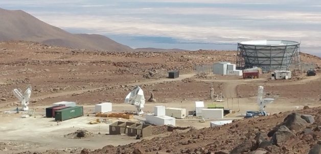
LBL The Simons Array in the Atacama in Chile, with the  Atacama Cosmology Telescope
The Simons Array will be located in Chile’s High Atacama Desert, at an elevation of about 17,000 feet. The site currently hosts the Atacama Cosmology Telescope (bowl-shaped structure at upper right) and the Simons Array (the three telescopes at bottom left, center and right). The Simons Observatory will merge these two experiments, add several new telescopes and set the stage for a next-generation experiment. (Credit: University of Pennsylvania)

The Simons Foundation has given $38.4 million to establish a new astronomy facility in Chile’s Atacama Desert, adding new telescopes and detectors alongside existing instruments in order to boost ongoing studies of the evolution of the universe, from its earliest moments to today. The Heising-Simons Foundation is providing an additional $1.7 million for the project.

The Simons Observatory is a collaboration among the U.S. Department of Energy’s Lawrence Berkeley National Laboratory (Berkeley Lab); UC Berkeley; Princeton University; the University of California at San Diego; and University of Pennsylvania, all of which are also providing financial support.

The project manager for the Simons Observatory will be located at Princeton, and Princeton faculty also will oversee the development, design, testing and manufacture of many of the observatory’s camera components.

The observatory will probe the subtle properties of the universe’s first light, known as cosmic microwave background (CMB) radiation.

A critical element in wringing new cosmological information from the CMB — which is the glow of heat left over from the Big Bang — is the use of densely packed, very sensitive cryogenic detectors. Princeton’s expertise with the detector development for the Atacama Cosmology Telescope in Chile and other observatories will complement the collaborative effort of the Simons Observatory, said Suzanne Staggs, Princeton’s project lead for the observatory and the Henry DeWolf Smyth Professor of Physics.

Of particular importance is the University’s large dilution refrigerator-based camera testing facility located in the Department of Physics. The CMB has a temperature of 3 degrees Kelvin (-454.27 degrees Fahrenheit), and CMB detectors are more sensitive the colder they are. The Princeton facility will test the Simons Observatory equipment at a frosty 80 millikelvin, or eighty one-thousandths of a degree above absolute zero.

Cosmic Microwave Background per ESA/Planck

ESA/Planck
ESA/Planck

The observatory will pay particular attention to the polarization, or directional information, in the CMB light to better understand what took place a fraction of a second after the Big Bang. While these events are hidden from view behind the glare of the microwave radiation, the disturbances they caused in the fabric of space-time affected the microwave’s polarization, and scientists hope to work backwards from these measurements to test theories about how the universe came into existence.

“The Simons Observatory will allow us to peer behind the dust in our galaxy and search for a true signal from the Big Bang,” said Adrian Lee, a physicist at Berkeley Lab, a UC Berkeley physics professor and one of the lead investigators at the observatory.

A key goal of the project is to detect gravitational waves generated by cosmic inflation, an extraordinarily rapid expansion of space that, according to the most popular cosmological theory, took place in an instant after the Big Bang. These primordial gravitational waves induced a very small but characteristic polarization pattern, called B-mode polarization, in the microwave background radiation that can be detected by telescopes and cameras like those planned for the Simons Observatory.

“While patterns that we see in the microwave sky are a picture of the structure of the universe 380,000 years after the Big Bang, we believe that some of these patterns were generated much earlier, by gravitational waves produced in the first moments of the universe’s expansion,” said project spokesperson Mark Devlin, a cosmologist at the University of Pennsylvania who leads the university’s team in the collaboration. “By measuring how the gravitational waves affect electrons and matter 380,000 years after the Big Bang we are observing fossils from the very, very early universe.”

Lee added, “Once we see the signal of inflation, it will be the beginning of a whole new era of cosmology.” We will then be looking at a time when the energy scale in the universe was a trillion times higher than the energy accessible in any particle accelerator on Earth.

By measuring how radiation from the early universe changed as it traveled through space to Earth, the observatory also will teach us about the nature of dark energy and dark matter, the properties of neutrinos and how large-scale structure formed as the universe expanded and evolved.

Two existing instruments at the site—the Atacama Cosmology Telescope and the Simons Array—are currently measuring this polarization. The foundation funds will merge these two experiments, expand the search and develop new technology for a fourth-stage, next-generation project—dubbed CMB-Stage 4 or CMB-S4—that could conceivably mine all the cosmological information in the cosmic microwave background fluctuations possible from a ground-based observatory.

“We are still in the planning stage for CMB-S4, and this is a wonderful opportunity for the foundations to create a seed for the ultimate experiment,” said Akito Kusaka, a Berkeley Lab physicist and one of the lead investigators. “This gets us off to a quick start.”

The Simons Observatory is designed to be a first step toward CMB-S4. This next-generation experiment builds on years of support from the National Science Foundation (NSF), and the Department of Energy (DOE) Office of Science has announced its intent to participate in CMB-S4, following the recommendation by its particle physics project prioritization panel [FNAL P5]. Such a project is envisioned to have telescopes at multiple sites and draw together a broad community of experts from the U.S. and abroad. The Atacama site in Chile has already been identified as an excellent location for CMB-S4, and the Simons Foundation funding will help develop it for that role.

“We are hopeful that CMB-S4 would shed light not only on inflation, but also on the dark elements of the universe: neutrinos and so-called dark energy and dark matter,” Kusaka said. “The nature of these invisible elements is among the biggest questions in particle physics as well.”

Beyond POLARBEAR

Experiments at the Chilean site have already paved the way for CMB-S4. A 2012 UC Berkeley-led experiment with participation by Berkeley Lab researchers, called POLARBEAR, used a 3.5-meter telescope at the Chilean site to measure the gravitational-lensing-generated B-mode polarization of the cosmic microwave background radiation.

POLARBEAR McGill Telescope located in the Atacama Desert of northern Chile in the Antofagasta Region. The POLARBEAR experiment is mounted on the Huan Tran Telescope (HTT) at the James Ax Observatory in the Chajnantor Science Reserve.

Team scientists confirmed in 2014 that the signal was strong enough to allow them eventually to measure the neutrino mass and the evolution of dark energy.

The recent addition of two more telescopes upgrades POLARBEAR to the Simons Array, which will speed up the mapping of the CMB and improve sky and frequency coverage. The $40 million in new funding will make possible the successor to the Simons Array and the nearby Atacama Cosmology Telescope.

Current stage-3 experiments for these short-wavelength microwaves, which must be chilled to three-tenths of a degree Kelvin above absolute zero, have about 10,000 pixels, Lee said.

“We need to make a leap in our technology to pave the way for the 500,000 detectors required for the ultimate experiment,” he said. “We’ll be generating the blueprint for a much more capable telescope.”

“The generosity of this award is unprecedented in our field, and will enable a major leap in scientific capability,” said Brian Keating, leader of the UC San Diego contingent and current project director. “People are used to thinking about mega- or gigapixel detectors in optical telescopes, but for signals in the microwave range 10,000 pixels is a lot. What we’re trying to do—the real revolution here—is to pave the way to increase our pixels number by more than an order of magnitude.”

Berkeley Lab and UC Berkeley will contribute $1.25 million in matching funds to the project over the next five years. The $1.7 million contributed by the Heising-Simons Foundation will be devoted to supporting research at Berkeley to improve the microwave detectors and to develop fabrication methods that are more efficient and cheaper, with the goal of boosting the number of detectors in CMB experiments by more than a factor of a 10.

The site in Chile is located in the Parque Astronómico, which is administered by the Comisión Nacional de Investigación Científica y Tecnológica (CONICYT). Since 1998, U.S. investigators and the NSF have worked with Chilean scientists, the University of Chile, and CONICYT to locate multiple projects at this high, dry site to study the CMB.

See the full LBL article here .

See the full Princeton article here .

Please help promote STEM in your local schools.

STEM Icon

Stem Education Coalition

A U.S. Department of Energy National Laboratory Operated by the University of California

University of California Seal

DOE Seal

From LBL: “Scientists Take a Major Leap Toward a ‘Perfect’ Quantum Metamaterial”

Berkeley Logo

Berkeley Lab

May 11, 2016
Glenn Roberts Jr.
510-486-5582

Berkeley Lab, UC Berkeley researchers lead study that uses trapped atoms in an artificial crystal of light

1
The wavelike pattern at the top shows the accordion-like structure of a proposed quantum material—an artificial crystal made of light—that can trap atoms in regularly spaced nanoscale pockets. These pockets can be made to hold a large collection of ultracold “host” atoms (green), slowed to a standstill by laser light, and individually planted “probe” atoms (red) that can be made to transmit quantum information in the form of a photon (particle of light). The lower panel shows how the artificial crystal can be reconfigured with light from an open (hyperbolic, in orange) geometry to a closed (elliptical, in green) geometry, which greatly affects the speed at which the probe atom can release a photon. (Credit: Pankaj K. Jha/UC Berkeley)

Scientists have devised a way to build a “quantum metamaterial”—an engineered material with exotic properties not found in nature—using ultracold atoms trapped in an artificial crystal composed of light. The theoretical work represents a step toward manipulating atoms to transmit information, perform complex simulations or function as powerful sensors.

The research team, led by scientists at the Department of Energy’s Lawrence Berkeley National Laboratory (Berkeley Lab) and UC Berkeley, proposes the use of an accordion-like atomic framework, or “lattice” structure, made with laser light to trap atoms in regularly spaced nanoscale pockets. Such a light-based structure, which has patterned features that in some ways resemble those of a crystal, is essentially a “perfect” structure—free of the typical defects found in natural materials.

Researchers believe they can pinpoint the placement of a so-called “probe” atom in this crystal of light, and actively tune its behavior with another type of laser light (near-infrared light) to make the atom cough up some of its energy on demand in the form of a particle of light, or photon.

This photon, in turn, can be absorbed by another probe atom (in the same or different lattice site) in a simple form of information exchange—like spoken words traveling between two string-connected tin cans.

“Our proposal is very significant,” said Xiang Zhang, director of Berkeley Lab’s Materials Sciences Division who led the related research paper*, published in April in Physical Review Letters. “We know that the enhancement and ultrafast control of single-photon emission lies at the heart of quantum technologies, in particular quantum information processing, and this is exactly what we have achieved here. Previous proposals can do one or the other but not both simultaneously.”

Zhang is also a professor at UC Berkeley, director of the National Science Foundation’s Center for Scalable and Integrated Nanomanufacturing and a member of the Kavli Energy NanoScience Institute at Berkeley Lab and UC Berkeley.

Pankaj K. Jha, a UC Berkeley postdoctoral researcher who is the lead author of the paper and works in Zhang’s group, said, “Now we have control over the speed of the release of a photon, so we can optically process information much faster, and efficiently transfer it from one point to another.” Other scientists who contributed to this work include Michael Mrejen, Jeongmin Kim, Chihhui Wu, Yuan Wang and Yuri V. Rostovtsev.

This ability to release a photon at fast rates, and to transmit it with low losses from one atom to another, is a vital step in processing information for quantum computation, which could use an array of these controlled photon releases to carry out complex calculations far more rapidly than is possible in modern computers.

A quantum computer, which the tech industry and scientific community are hotly pursuing because of its potential to perform more complex calculations than are possible using modern supercomputers, could tap into the bizarre quantum realm in which ordinary physics rules don’t apply.

While today’s computers can store information as binary bits—either ones or zeroes—a quantum compter would use “qubits” in which an individual bit of information can simultaneously exist in multiple states. These qubits could take the form of atoms, photons, electrons, or even as an individual fundamental property of a particle, and would exponentially increase the number of calculations a computer could perform in an instant.

The non-uniform distribution of the ultracold atoms in the artificial crystal is a key to this latest study, said Jha. “It makes the crucial difference for creating a ‘perfectly’ lossless and reconfigurable quantum metamaterial,” he said, allowing the optical structure of the artificial crystal to be reconfigured from an open geometry (hyperbolic-shaped) to a closed one (elliptical) at the same frequency and with ultrafast timing. This controllable shape-change dramatically changes the speed at which a probe atom in the artificial crystal releases a photon.

The latest proposal suggests that it is possible to speed up the rate at which a probe atom can emit a photon from nanoseconds, or billionths of a second, to picoseconds, or trillionths of a second. Also, this process is importantly considered “lossless,” meaning the photons would not lose any of their energy to their surrounding structure as they likely would in a traditional material. This overcomes one hurdle toward quantum computing and information processing.

Atoms planted in the artificial crystal could also possibly be induced to hop from one place to another. In this case, the atoms could themselves serve as the information carriers in a quantum computer or be arranged as quantum sensors, Jha said.

Jha noted that this latest study marries metamaterials research with the science of “cold atoms,” which are atoms that have been slowed and even brought to a standstill using laser light, which in the process chills them to supercool temperatures. He said, “This integration has solved some of the outstanding challenges for metamaterial platforms and outperforms other designs in several key aspects crucial for quantum technologies.”

The researchers found that rubidium atoms are ideally suited for this study, however barium, calcium and cesium atoms can also be trapped or planted in the artificial crystal, as they exhibit similar energy levels. While the artificial crystal used in the study is described as one-dimensional, Jha said the same approach could be easily extended to create 2-D and 3-D quantum metamaterial crystal structures out of light.

To realize the proposed metamaterial in an actual experiment, Zhang and Jha said the research team would need to trap several atoms per lattice site in the artificial crystal, and to hold those atoms in the lattice even when they are excited to higher energy states.

Zhang said, “Berkeley Lab has been a leader in groundbreaking research in metamaterials, and this work could open new realms of opportunities for quantum light-matter interactions, with enticing applications in quantum information science.”

Jha added, “We believe that the combination of these two contemporary realms of science will help to address key challenges in both fields and open an entirely new research direction at the interface of quantum photonics and artificial materials.”

The work was supported by the U.S. Air Force Office of Scientific Research and the Gordon and Betty Moore Foundation.

View more work by Xiang Zhang’s laboratory: http://xlab.me.berkeley.edu/.

*Science paper:
Coherence-Driven Topological Transition in Quantum Metamaterials

See the full article here .

Please help promote STEM in your local schools.

STEM Icon

Stem Education Coalition

A U.S. Department of Energy National Laboratory Operated by the University of California

University of California Seal

DOE Seal

From LBL: “Seeing Atoms and Molecules in Action with an Electron ‘Eye’ “

Berkeley Logo

Berkeley Lab

April 26, 2016
Glenn Roberts Jr.
510-486-5582
geroberts@lbl.gov

1
Daniele Filippetto, a Berkeley Lab scientist, works on the High-Repetition-rate Electron Scattering apparatus (HiRES), which will function like an ultrafast electron camera. HiRES is a new capability that builds on the Advanced Photo-injector Experiment (APEX), a prototype electron source for advanced X-ray lasers. (Roy Kaltschmidt/Berkeley Lab)

A unique rapid-fire electron source—originally built as a prototype for driving next-generation X-ray lasers—will help scientists at the Department of Energy’s Lawrence Berkeley National Laboratory (Berkeley Lab) study ultrafast chemical processes and changes in materials at the atomic scale. This could provide new insight in how to make materials with custom, controllable properties and improve the efficiency and output of chemical reactions.

This newly launched setup, dubbed HiRES (for High Repetition-rate Electron Scattering apparatus), will function like an ultrafast electron camera, potentially producing images that can pinpoint defects and their effects, track electronic and superconducting properties in exotic materials, and detail chemical reactions in gases, liquids and biological samples that are difficult to study using more conventional, X-ray-based experiments.

The new research tool produces highly focused electron bunches, each containing up to 1 million electrons. The electrons stream at a rate of up to 1 million bunches per second, or 1 trillion electrons per second.

Electrons will be used as a fast camera shutter to capture snapshots of samples as they change over femtoseconds, or quadrillionths of a second. An initial laser pulse will trigger a reaction in the sample that is followed an instant later by an electron pulse to produce an image of that reaction.

HiRES delivered its first electron beam March 28 and experiments are set to begin in May.

Daniele Filippetto, a Berkeley Lab scientist who is leading HiRES, has for much of his scientific career focused on building electron sources, also called “electron guns,” that can drive advanced X-ray lasers known as “free-electron lasers.” These electron guns are designed to produce a chain of high-energy electron pulses that are accelerated and then forced by powerful magnetic fields to give up some of their energy in the form of X-ray light.

SACLA Free-Electron Laser Riken Japan

Free-electron lasers have opened new frontiers in studying materials and chemistry at the nanoscale and beyond, and Filippetto said he hopes to pave new ground with HiRES, too, using a technique known as “ultrafast electron diffraction,” or UED, that is similar to X-ray diffraction.

In these techniques, a beam of X-rays or electrons hits a sample, and the scattering of X-rays or electrons is collected on a detector. This pattern, known as a diffraction pattern, provides structural information about the sample. X-rays and electrons interact differently: electrons scatter from a sample’s electrons and the atoms’ nuclei, for example, while X-rays scatter only from the electrons.

The unique electron gun that Filippetto and his team are using is a part of Berkeley Lab’s APEX (Advanced Photo-injector EXperiment), which has served as a prototype system for LCLS-II, a next-generation X-ray laser project underway at SLAC National Acceleratory Laboratory in Menlo Park, Calif. Berkeley Lab is a member of the LCLS-II project collaboration.

“The APEX gun is a unique source of ultrafast electrons, with the potential to reach unprecedented precision and stability in timing—ultimately at or below 10 femtoseconds,” Filippetto said. “With HiRES, the time resolution will be about 100 femtoseconds, or the time it takes for chemical bonds to form and break. So you can look at the same kinds of processes that you can look at with an X-ray free-electron laser, but with an electron eye.”

He added, “You can see the structure and the relative distances between atoms in a molecule changing over time across the whole structure. You need fewer electrons than X-rays to get an image, and in principal there can be much less damage to the sample with electrons.”

2
This computerized rendering shows the layout of the HiRES ultrafast electron diffraction beamline, which is located in the domed Advanced Light Source building at Berkeley Lab. At left (on blue base) is APEX, the electron source for HiRES. (Courtesy of Daniele Filippetto/Berkeley Lab)

Filippetto in 2014 received a five-year DOE Early Career Research Program award that is supporting his work on HiRES. The work is also supported by the Berkeley Lab Laboratory Directed Research and Development Program.

Already, Berkeley Lab has world-class research capabilities in other electron-beam microscopic imaging techniques, in building nanostructures, and in a range of X-ray experimental techniques, Filippetto noted. All of these capabilities are accessible to the world’s scientists via the lab’s Molecular Foundry and Advanced Light Source (ALS).

“If we couple all of these together with the power of HiRES, then you basically can collect full information from your samples,” he said. “You can get static images with subatomic resolution, the ultrafast structural response, and chemical information about a sample—in the same lab and in the same week.”

3
A view of the HiRES ultrafast electron diffraction (UED) beamline at Berkeley Lab’s APEX. (Roy Kaltschmidt/Berkeley Lab)

Filippetto has a goal to improve the focus of the HiRES electron beam from microns, or millionths of a meter in diameter, to the nanometer scale (billionths of a meter), and to also improve the timing from hundredths of femtoseconds to tens of femtoseconds to boost the quality of the images it produces and also to study even faster processes at the atomic scale.

Andrew Minor, director of the Molecular Foundry’s National Center for Electron Microscopy said he is excited about the potential for HiRES to ultimately study the structure of single molecules and to explore the propagation of microscopic defects in materials at the speed of sound.

“We want to study nanoscale processes such as the structural changes in a material as a crack moves through it at the speed of sound,” he said. Also, the timing of HiRES may allow scientists to study real-time chemical reactions in an operating battery, he added.

“What is really interesting to me is that you can potentially focus the beam down to a small size, and then you would really have a system that competes with X-ray free-electron lasers,” Minor said, which opens up the possibility of electron imaging of single biological particles.

He added, “I think there is a very large unexplored space in terms of using electrons at the picosecond (trillionths of a second) and nanosecond (billionths off a second) time scales to directly image materials.”

There are tradeoffs in using X-rays vs. electrons to study ultrafast processes at ultrasmall scales, he noted, though “even if the capabilities are similar, it’s worth pursuing” because of the smaller size and lesser cost of machines like APEX and HiRES compared to X-ray free-electron lasers.

Scientists from Berkeley Lab’s Materials Sciences Division and from UC Berkeley will conduct the first set of experiments using HiRES, Filippetto said, including studies of the structural and electronic properties of single-layer and multilayer graphene, as well as other materials with semiconductor and superconductor properties.

There are also some clear uses for HiRES in chemistry and biology experiments, Filippetto noted. “The idea is to push things to see ever-more-complicated structures and to open the doors to all of the possible applications,” he said.

There are plans to forge connections between HiRES and other lab facilities, like the ALS, where HiRES is located, and the lab’s National Center for Electron Microscopy at the Molecular Foundry.

“Already, we are working with the microscopy center on the first experiments,” Filippetto added. “We are adapting the microscope’s sample holder so that one can easily move samples from one instrument to another.”

Filippetto said there are discussions with ALS scientists on the possibility of gathering complementary information from the same samples using both X-rays from the ALS and electrons from HiRES.

“This would make HiRES more accessible to a larger scientific community,” he added.

The Molecular Foundry and Advanced Light Source are DOE Office of Science User Facilities. HiRES is supported by the U.S. Department of Energy Office of Science.

LBL Advanced Light Source

4
A labeled diagram showing the components of the HiRES beamline at Berkeley Lab. (Courtesy of Daniele Filippetto/Berkeley Lab)

See the full article here .

Please help promote STEM in your local schools.

STEM Icon

Stem Education Coalition

A U.S. Department of Energy National Laboratory Operated by the University of California

University of California Seal

DOE Seal

From Symmetry: “Physicists build ultra-powerful accelerator magnet”

Symmetry Mag

Symmetry

04/07/16
Sarah Charley

Magnet built for LHC

The next generation of cutting-edge accelerator magnets is no longer just an idea. Recent tests revealed that the United States and CERN have successfully co-created a prototype superconducting accelerator magnet that is much more powerful than those currently inside the Large Hadron Collider.

CERN LHC Map
CERN LHC Grand Tunnel
CERN LHC particles
CERN/LHC

Engineers will incorporate more than 20 magnets similar to this model into the next iteration of the LHC, which will take the stage in 2026 and increase the LHC’s luminosity by a factor of ten. That translates into a ten-fold increase in the data rate.

“Building this magnet prototype was truly an international effort,” says Lucio Rossi, the head of the High-Luminosity (HighLumi) LHC project at CERN. “Half the magnetic coils inside the prototype were produced at CERN, and half at laboratories in the United States.”

During the original construction of the Large Hadron Collider, US Department of Energy national laboratories foresaw the future need for stronger LHC magnets and created the LHC Accelerator Research Program (LARP): an R&D program committed to developing new accelerator technology for future LHC upgrades.

MQXF1 quadrupole 1.5-meter prototype magnet sits at Fermilab before testing.
MQXF1 quadrupole 1.5-meter prototype magnet sits at Fermilab before testing. G. Ambrosio (US-LARP and Fermilab), P. Ferracin and E. Todesco (CERN TE-MSC)

This 1.5-meter-long model, which is a fully functioning accelerator magnet, was developed by scientists and engineers at Fermilab [FNAL], Brookhaven National Laboratory [BNL], Lawrence Berkeley National Laboratory [LBL], and CERN.

FNAL II photo
FNAL

BNL Logo (2)
BNL

LBL Big
LBL

CERN
CERN

The magnet recently underwent an intense testing program at Fermilab, which it passed in March with flying colors. It will now undergo a rigorous series of endurance and stress tests to simulate the arduous conditions inside a particle accelerator.

This new type of magnet will replace about 5 percent of the LHC’s focusing and steering magnets when the accelerator is converted into the High-Luminosity LHC, a planned upgrade which will increase the number and density of protons packed inside the accelerator. The HL-LHC upgrade will enable scientists to collect data at a much faster rate.

The LHC’s magnets are made by repeatedly winding a superconducting cable into long coils. These coils are then installed on all sides of the beam pipe and encased inside a superfluid helium cryogenic system. When cooled to 1.9 Kelvin, the coils can carry a huge amount of electrical current with zero electrical resistance. By modulating the amount of current running through the coils, engineers can manipulate the strength and quality of the resulting magnetic field and control the particles inside the accelerator.

The magnets currently inside the LHC are made from niobium titanium, a superconductor that can operate inside a magnetic field of up to 10 teslas before losing its superconducting properties. This new magnet is made from niobium-three tin (Nb3Sn), a superconductor capable of carrying current through a magnetic field of up to 20 teslas.

“We’re dealing with a new technology that can achieve far beyond what was possible when the LHC was first constructed,” says Giorgio Apollinari, Fermilab scientist and Director of US LARP. “This new magnet technology will make the HL-LHC project possible and empower physicists to think about future applications of this technology in the field of accelerators.”

High-Luminosity LHC coil
High-Luminosity LHC coil similar to those incorporated into the successful magnet prototype shows the collaboration between CERN and the LHC Accelerator Research Program, LARP.
Photo by Reidar Hahn, Fermilab

This technology is powerful and versatile—like upgrading from a moped to a motorcycle. But this new super material doesn’t come without its drawbacks.

“Niobium-three tin is much more complicated to work with than niobium titanium,” says Peter Wanderer, head of the Superconducting Magnet Division at Brookhaven National Lab. “It doesn’t become a superconductor until it is baked at 650 degrees Celsius. This heat-treatment changes the material’s atomic structure and it becomes almost as brittle as ceramic.”

Building a moose-sized magnet from a material more fragile than a teacup is not an easy endeavor. Scientists and engineers at the US national laboratories spent 10 years designing and perfecting a new and internationally reproducible process to wind, form, bake and stabilize the coils.

“The LARP-CERN collaboration works closely on all aspects of the design, fabrication and testing of the magnets,” says Soren Prestemon of the Berkeley Center for Magnet Technology at Berkeley Lab. “The success is a testament to the seamless nature of the collaboration, the level of expertise of the teams involved, and the ownership shown by the participating laboratories.”

This model is a huge success for the engineers and scientists involved. But it is only the first step toward building the next big supercollider.

“This test showed that it is possible,” Apollinari says. “The next step is it to apply everything we’ve learned moving from this prototype into bigger and bigger magnets.”

See the full article here .

Please help promote STEM in your local schools.

STEM Icon

Stem Education Coalition

Symmetry is a joint Fermilab/SLAC publication.


From LBL: “Scientists Push Valleytronics One Step Closer to Reality”

Berkeley Logo

Berkeley Lab

April 4, 2016
Dan Krotz
510-486-4019
dakrotz@lbl.gov

Scientists with the U.S. Department of Energy’s Lawrence Berkeley National Laboratory (Berkeley Lab) have taken a big step toward the practical application of “valleytronics,” which is a new type of electronics that could lead to faster and more efficient computer logic systems and data storage chips in next-generation devices.

As reported online April 4 in the journal Nature Nanotechnology, the scientists experimentally demonstrated, for the first time, the ability to electrically generate and control valley electrons in a two-dimensional semiconductor.

1
This schematic shows a TMDC monolayer coupled with a host ferromagnetic semiconductor, which is an experimental approach developed by Berkeley Lab scientists that could lead to valleytronic devices. Valley polarization can be directly determined from the helicity of the emitted electroluminescence, shown by the orange arrow, as a result of electrically injected spin-polarized holes to the TMDC monolayer, shown by the blue arrow. The black arrow represents the direction of the applied magnetic field. (Credit: Berkeley Lab)

Valley electrons are so named because they carry a valley “degree of freedom.” This is a new way to harness electrons for information processing that’s in addition to utilizing an electron’s other degrees of freedom, which are quantum spin in spintronic devices and charge in conventional electronics.

More specifically, electronic valleys refer to the energy peaks and valleys in electronic bands. A two-dimensional semiconductor called transition metal dichalcogenide (TMDC) has two distinguishable valleys of opposite spin and momentum. Because of this, the material is suitable for valleytronic devices, in which information processing and storage could be carried out by selectively populating one valley or another.

However, developing valleytronic devices requires the electrical control over the population of valley electrons, a step that has proven very challenging to achieve so far.

Now, Berkeley Lab scientists have experimentally demonstrated the ability to electrically generate and control valley electrons in TMDCs. This is an especially important advance because TMDCs are considered to be more “device ready” than other semiconductors that exhibit valleytronic properties.

“This is the first demonstration of electrical excitation and control of valley electrons, which will accelerate the next generation of electronics and information technology,” says Xiang Zhang, who led this study and who is the director of Berkeley Lab’s Materials Sciences Division.

Zhang also holds the Ernest S. Kuh Endowed Chair at the University of California (UC) Berkeley and is a member of the Kavli Energy NanoSciences Institute at Berkeley. Several other scientists contributed to this work, including Yu Ye, Jun Xiao, Hailong Wang, Ziliang Ye, Hanyu Zhu, Mervin Zhao, Yuan Wang, Jianhua Zhao and Xiaobo Yin.

3
From left, Xiang Zhang, Yu Ye, Jun Xiao, and Yuan Wang are part of a team of scientists that made a big advance in valleytronics.

Their research could lead to a new type of electronics that utilize all three degrees of freedom—charge, spin, and valley, which together could encode an electron with eight bits of information instead of two in today’s electronics. This means future computer chips could process more information with less power, enabling faster and more energy efficient computing technologies.

“Valleytronic devices have the potential to transform high-speed data communications and low-power devices,” says Ye, a postdoctoral researcher in Zhang’s group and the lead author of the paper.

The scientists demonstrated their approach by coupling a host ferromagnetic semiconductor with a monolayer of TMDC. Electrical spin injection from the ferromagnetic semiconductor localized the charge carriers to one momentum valley in the TMDC monolayer.

Importantly, the scientists were able to electrically excite and confine the charge carriers in only one of two sets of valleys. This was achieved by manipulating the injected carrier’s spin polarizations, in which the spin and valley are locked together in the TMDC monolayer.

The two sets of valleys emit different circularly polarized light. The scientists observed this circularly polarized light, which confirmed they had successfully electrically induced and controlled valley electrons in TMDC.

“Our research solved two main challenges in valleytronic devices. The first is electrically restricting electrons to one momentum valley. The second is detecting the resulting valley-polarized current by circular polarized electroluminescence,” says Ye. “Our direct electrical generation and control of valley charge carriers, in TMDC, opens up new dimensions in utilizing both the spin and valley degrees of freedom for next-generation electronics and computing.”

The research was supported by the Office of Naval Research Multidisciplinary University Research Initiative program, the National Science Foundation, China’s Ministry of Science and Technology, and the National Science Foundation of China.

See the full article here .

Please help promote STEM in your local schools.

STEM Icon

Stem Education Coalition

A U.S. Department of Energy National Laboratory Operated by the University of California

University of California Seal

DOE Seal