
From The DOE’s Lawrence Berkeley National Laboratory
2.15.23
Rachel Berkowitz
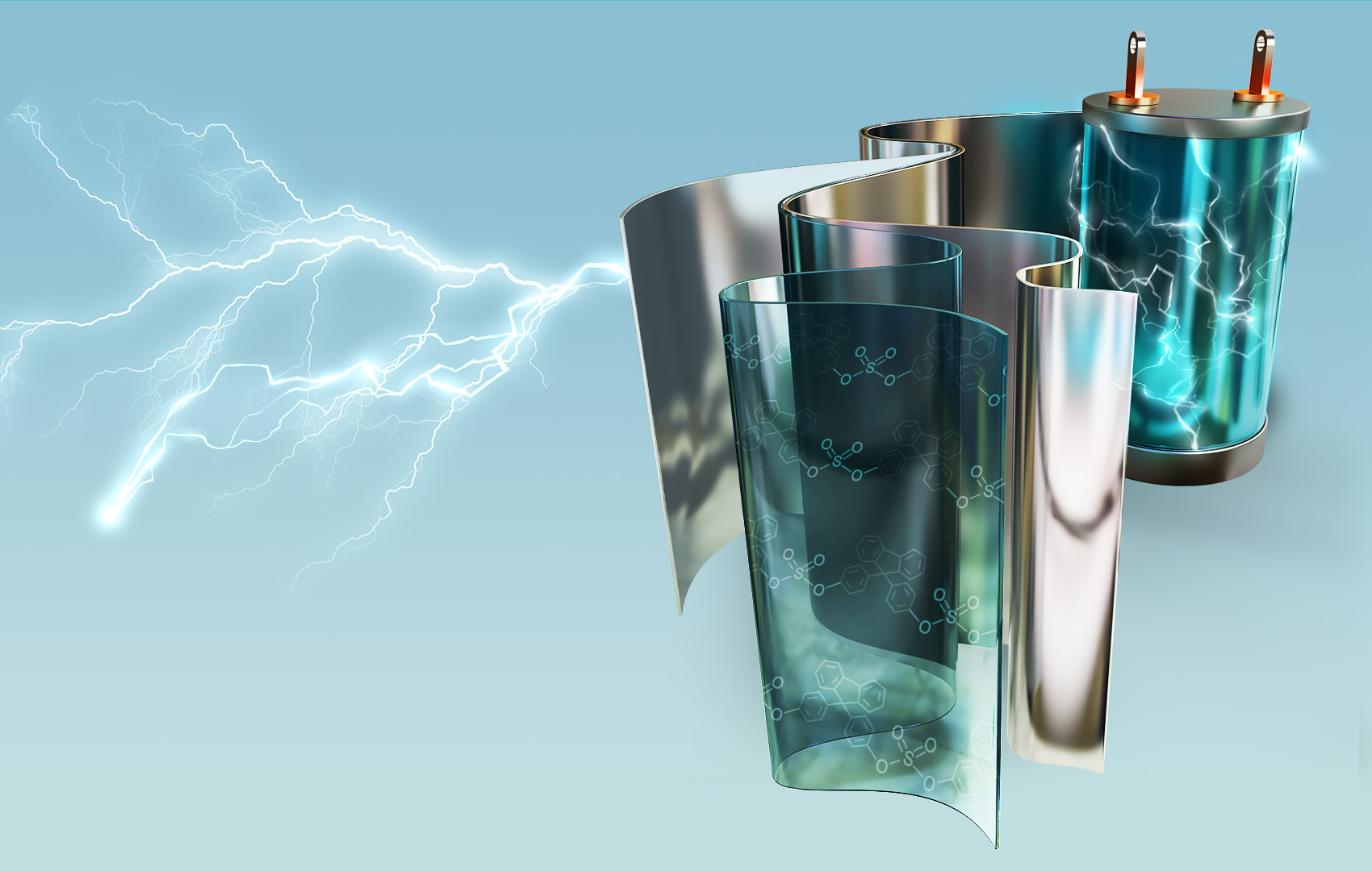
A new type of polysulfate compound can be used to make polymer film capacitors that store and discharge high density of electrical energy while tolerating heat and electric fields beyond the limits of existing polymer film capacitors. (Credit: Yi Liu and He (Henry) Li/Berkeley Lab)
Flexible polymers made with a new generation of the Nobel-winning “click chemistry” reaction find use in capacitors and other applications.
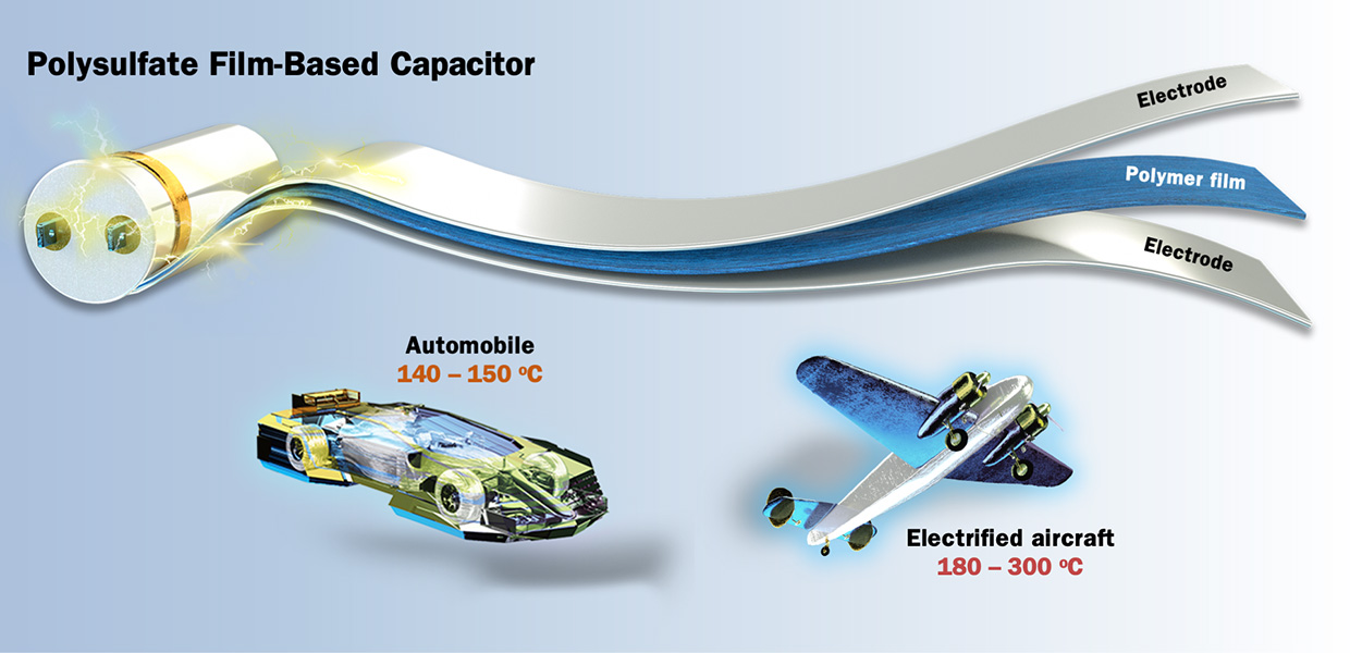
Society’s growing demand for high-voltage electrical technologies – including pulsed power systems, cars and electrified aircraft, and renewable energy applications – requires a new generation of capacitors that store and deliver large amounts of energy under intense thermal and electrical conditions. Researchers at the Department of Energy’s Lawrence Berkeley National Laboratory (Berkeley Lab) and Scripps Research have now developed a new polymer-based device that efficiently handles record amounts of energy while withstanding extreme temperatures and electric fields. The device is composed of materials synthesized via a next-generation version of the chemical reaction for which three scientists won the 2022 Nobel Prize in Chemistry.
Polymer film capacitors are electrical components that store and release energy within an electric field using a thin plastic layer as the insulating layer. They make up 50% of the global high voltage capacitor market and offer advantages including light weight, low cost, mechanical flexibility, and robust cyclability. But state-of-the-art polymer film capacitors decrease dramatically in performance with increasing temperature and voltages. Developing new materials with improved tolerance for heat and electric fields is paramount; and creating polymers with near-perfect chemistry offers a way to do so.
“Our work adds a new class of electrically robust polymers to the table. It opens many possibilities to the exploration of more robust, high performing materials,” said Yi Liu, a chemist at Berkeley Lab and senior author on the Joule [below] study reporting the work. Liu is the Facility Director of Organic and Macromolecular Synthesis at the Molecular Foundry [below], a DOE Office of Science user facility at Berkeley Lab.
In addition to remaining stable when subjected to high temperatures, a capacitor needs to be a strong “dielectric” material, meaning that it remains a strong insulator when subjected to high voltages. However, few known materials systems exist that deliver both thermal stability and dielectric strength. This scarcity is due to a lack of reliable and convenient synthesis methods, as well as a lack of fundamental understanding of the relationship between polymer structure and properties. “Improving the thermal stability of existing films while retaining their electrical insulating strength is an ongoing materials challenge,” said Liu.
A long-term collaboration between researchers at the Molecular Foundry and Scripps Research Institute has now met that challenge. They used a simple and quick chemical reaction developed in 2014 that swaps out fluorine atoms in compounds that contain sulfur-fluoride bonds, to yield long polymer chains of sulfate molecules called polysulfates. This Sulfur-Fluoride Exchange (SuFEx) reaction is a next-generation version of the click chemistry reaction pioneered by K. Barry Sharpless, a chemist at Scripps Research and two-time Nobel laureate in Chemistry, along with Peng Wu, also a chemist at Scripps Research. The near-perfect yet easy-to-run reactions join separate molecular entities through strong chemical bonds that form between different reactive groups. Liu’s team had originally used a variety of thermal analysis tools to examine the basic thermal and mechanical properties of these new materials.
Polysulfates with excellent thermal properties are casted into flexible free-standing films. High-temperature, high-voltage capacitors based on such films show state-of-the-art energy storage properties at 150 degrees Celsius. Such power capacitors are promising for improving the energy efficiency and reliability of integrated power systems in demanding applications such as electrified transportation. (Credit: Yi Liu and He (Henry) Li/Berkeley Lab)
As part of a Berkeley Lab program to synthesize and identify novel materials that could be useful in energy storage, Liu and his colleagues now find that, surprisingly, the polysulfates have outstanding dielectric properties, especially at high electric fields and temperatures. “Several commercial and lab-generated polymers are known for their dielectric properties, but polysulfates had never been considered. The marriage between polysulfates and dielectrics is one of the novelties here,” said He Li, a postdoctoral researcher in the Molecular Foundry and in Berkeley Lab’s Materials Sciences Division, and lead author of the study.
Inspired by the excellent baseline dielectric properties offered by polysulfates, the researchers deposited extremely thin layers of aluminum oxide (Al2O3) onto thin films of the material to engineer capacitor devices with enhanced energy storage performance. They discovered that the fabricated capacitors exhibited excellent mechanical flexibility, withstood electric fields of more than 750 million volts per meter, and performed efficiently at temperatures up to 150 degrees Celsius. In comparison, today’s benchmark commercial polymer capacitors only function reliably at temperatures lower than 120 degrees Celsius. Above that temperature, they can only withstand electric fields smaller than 500 million volts per meter, and the energy efficiency severely drops by over half.
The work opens new possibilities for exploring robust, high performing materials for energy storage. “We have provided deep insight into the underlying mechanisms that contribute to the material’s excellent performance,” said Wu.
The polymer strikes a balance of electrical, thermal, and mechanical properties, likely due to the sulfate linkages introduced by the click chemistry reaction. Because modular chemistry accommodates extraordinary structural diversity and scalability, the same route could offer a viable path to new polymers with higher performance that meet even more demanding operational conditions.
The polysulfates are strong contenders to become new state-of-the-art polymer dielectrics. Once researchers overcome barriers in large-scale manufacturing processes for thin film materials, the devices could greatly improve the energy efficiency of integrated power systems in electric vehicles and enhance their operational reliability.
“Who could have imagined that a wispy sulfate polymer film could fend off lightning and fire, two of the most destructive forces in the universe?!” said Sharpless.
“We’re continuously pushing the envelope of thermal and electrical properties, and accelerating the lab-to-market transition,” Liu added.
The technology is now available for licensing by contacting ipo@lbl.gov.
The work received funding from the Department of Energy’s Office of Science, the National Science Foundation, and the National Institute of Health. The work was carried out at the Molecular Foundry.
Graphical abstract

Figure 1. Chemical synthesis and electronic structure characterization

(A) Schematic of the polysulfates P1, P2, and P3 based on SuFEx click chemistry.
(B) Frequency-dependent dielectric spectra of dielectric constant (k) of polysulfates P1, P2, and P3 obtained at 30°C.
(C) Calculated density of states (DOS) and the corresponding computed electronic band gap of polysulfates P1, P2, and P3.
(D) Correlation between glass transition temperature and optical band gap of polysulfates P1, P2, and P3 and commercial aromatic dielectric polymers.[23]
All three polysulfates display desirable k values (e.g., 3.4–3.8 at 104 Hz) and low loss tangents (tan δ), as revealed by the frequency-dependent dielectric spectra (Figures 1B and S6). The experimental optical Eg values (obtained from UV-vis spectroscopy) are in the range between 4.36 and 3.90 eV and follow the order of P1 > P2 > P3, which agree favorably with the trend of the simulated electronic Eg values (obtained from density functional theory [DFT] calculations) (Figures 1C and S7–S9). When comparing the Eg and Tg values against the major commercial dielectric polymers containing aromatic repeat units, including PEEK, PEI, FPE, polyethylene terephthalate (PET), polyethylene naphthalate (PEN), polyamideimide (PAI), and PIs (Kapton PI and Upilex-S PI) (which follow an empirical inverse correlation between Eg and Tg), the polysulfates show an apparent deviation with decent Tg values despite their larger Eg values (Figures 1D and S10). In addition, the polysulfates P1–P3 display lower computed mass densities (∼1.10–1.20 g cm−3) than those of commercial dielectric polymers (Figure S11; Table S1). The combination of lightweight, wide Eg, large k, low tan δ, along with high Tg is likely essential for high-temperature film capacitor applications.
See the science paper for more instructive imagery.
See the full article here .
Comments are invited and will be appreciated, especially if the reader finds any errors which I can correct. Use “Reply”.

five-ways-keep-your-child-safe-school-shootings
Please help promote STEM in your local schools.
![]()


Bringing Science Solutions to the World
In the world of science, The Lawrence Berkeley National Laboratory (Berkeley Lab) is synonymous with “excellence.” Thirteen Nobel prizes are associated with Berkeley Lab. Seventy Lab scientists are members of the The National Academy of Sciences, one of the highest honors for a scientist in the United States. Thirteen of our scientists have won the National Medal of Science, our nation’s highest award for lifetime achievement in fields of scientific research. Eighteen of our engineers have been elected to the The National Academy of Engineering, and three of our scientists have been elected into The Institute of Medicine. In addition, Berkeley Lab has trained thousands of university science and engineering students who are advancing technological innovations across the nation and around the world.
Berkeley Lab is a member of the national laboratory system supported by The DOE through its Office of Science. It is managed by the University of California and is charged with conducting unclassified research across a wide range of scientific disciplines. Located on a 202-acre site in the hills above The University of California-Berkeley campus that offers spectacular views of the San Francisco Bay, Berkeley Lab employs approximately 3,232 scientists, engineers and support staff. The Lab’s total costs for FY 2014 were $785 million. A recent study estimates the Laboratory’s overall economic impact through direct, indirect and induced spending on the nine counties that make up the San Francisco Bay Area to be nearly $700 million annually. The Lab was also responsible for creating 5,600 jobs locally and 12,000 nationally. The overall economic impact on the national economy is estimated at $1.6 billion a year. Technologies developed at Berkeley Lab have generated billions of dollars in revenues, and thousands of jobs. Savings as a result of Berkeley Lab developments in lighting and windows, and other energy-efficient technologies, have also been in the billions of dollars.
Berkeley Lab was founded in 1931 by Ernest Orlando Lawrence, a University of California-Berkeley physicist who won the 1939 Nobel Prize in physics for his invention of the cyclotron, a circular particle accelerator that opened the door to high-energy physics. It was Lawrence’s belief that scientific research is best done through teams of individuals with different fields of expertise, working together. His teamwork concept is a Berkeley Lab legacy that continues today.
History
1931–1941
The laboratory was founded on August 26, 1931, by Ernest Lawrence, as the Radiation Laboratory of the University of California-Berkeley, associated with the Physics Department. It centered physics research around his new instrument, the cyclotron, a type of particle accelerator for which he was awarded the Nobel Prize in Physics in 1939.

LBNL 88 inch cyclotron.

Throughout the 1930s, Lawrence pushed to create larger and larger machines for physics research, courting private philanthropists for funding. He was the first to develop a large team to build big projects to make discoveries in basic research. Eventually these machines grew too large to be held on the university grounds, and in 1940 the lab moved to its current site atop the hill above campus. Part of the team put together during this period includes two other young scientists who went on to establish large laboratories; J. Robert Oppenheimer founded The DOE’s Los Alamos Laboratory, and Robert Wilson founded The DOE’s Fermi National Accelerator Laboratory.
1942–1950
Leslie Groves visited Lawrence’s Radiation Laboratory in late 1942 as he was organizing the Manhattan Project, meeting J. Robert Oppenheimer for the first time. Oppenheimer was tasked with organizing the nuclear bomb development effort and founded today’s Los Alamos National Laboratory to help keep the work secret. At the RadLab, Lawrence and his colleagues developed the technique of electromagnetic enrichment of uranium using their experience with cyclotrons. The “calutrons” (named after the University) became the basic unit of the massive Y-12 facility in Oak Ridge, Tennessee. Lawrence’s lab helped contribute to what have been judged to be the three most valuable technology developments of the war (the atomic bomb, proximity fuse, and radar). The cyclotron, whose construction was stalled during the war, was finished in November 1946. The Manhattan Project shut down two months later.
1951–2018
After the war, the Radiation Laboratory became one of the first laboratories to be incorporated into the Atomic Energy Commission (AEC) (now The Department of Energy . The most highly classified work remained at Los Alamos, but the RadLab remained involved. Edward Teller suggested setting up a second lab similar to Los Alamos to compete with their designs. This led to the creation of an offshoot of the RadLab (now The DOE’s Lawrence Livermore National Laboratory) in 1952. Some of the RadLab’s work was transferred to the new lab, but some classified research continued at Berkeley Lab until the 1970s, when it became a laboratory dedicated only to unclassified scientific research.
Shortly after the death of Lawrence in August 1958, the UC Radiation Laboratory (both branches) was renamed the Lawrence Radiation Laboratory. The Berkeley location became the Lawrence Berkeley Laboratory in 1971, although many continued to call it the RadLab. Gradually, another shortened form came into common usage, LBNL. Its formal name was amended to Ernest Orlando Lawrence Berkeley National Laboratory in 1995, when “National” was added to the names of all DOE labs. “Ernest Orlando” was later dropped to shorten the name. Today, the lab is commonly referred to as “Berkeley Lab”.
The Alvarez Physics Memos are a set of informal working papers of the large group of physicists, engineers, computer programmers, and technicians led by Luis W. Alvarez from the early 1950s until his death in 1988. Over 1700 memos are available on-line, hosted by the Laboratory.
The lab remains owned by the Department of Energy , with management from the University of California. Companies such as Intel were funding the lab’s research into computing chips.
Science mission
From the 1950s through the present, Berkeley Lab has maintained its status as a major international center for physics research, and has also diversified its research program into almost every realm of scientific investigation. Its mission is to solve the most pressing and profound scientific problems facing humanity, conduct basic research for a secure energy future, understand living systems to improve the environment, health, and energy supply, understand matter and energy in the universe, build and safely operate leading scientific facilities for the nation, and train the next generation of scientists and engineers.
The Laboratory’s 20 scientific divisions are organized within six areas of research: Computing Sciences; Physical Sciences; Earth and Environmental Sciences; Biosciences; Energy Sciences; and Energy Technologies. Berkeley Lab has six main science thrusts: advancing integrated fundamental energy science; integrative biological and environmental system science; advanced computing for science impact; discovering the fundamental properties of matter and energy; accelerators for the future; and developing energy technology innovations for a sustainable future. It was Lawrence’s belief that scientific research is best done through teams of individuals with different fields of expertise, working together. His teamwork concept is a Berkeley Lab tradition that continues today.
Berkeley Lab operates five major National User Facilities for the DOE Office of Science:
The Advanced Light Source (ALS) is a synchrotron light source with 41 beam lines providing ultraviolet, soft x-ray, and hard x-ray light to scientific experiments.
 The DOE’s Lawrence Berkeley National Laboratory Advanced Light Source.
The ALS is one of the world’s brightest sources of soft x-rays, which are used to characterize the electronic structure of matter and to reveal microscopic structures with elemental and chemical specificity. About 2,500 scientist-users carry out research at ALS every year. Berkeley Lab is proposing an upgrade of ALS which would increase the coherent flux of soft x-rays by two-three orders of magnitude.
Berkeley Lab Laser Accelerator (BELLA) Center

The DOE Joint Genome Institute supports genomic research in support of the DOE missions in alternative energy, global carbon cycling, and environmental management. The JGI’s partner laboratories are Berkeley Lab, DOE’s Lawrence Livermore National Laboratory, DOE’s Oak Ridge National Laboratory (ORNL), DOE’s Pacific Northwest National Laboratory (PNNL), and the HudsonAlpha Institute for Biotechnology . The JGI’s central role is the development of a diversity of large-scale experimental and computational capabilities to link sequence to biological insights relevant to energy and environmental research. Approximately 1,200 scientist-users take advantage of JGI’s capabilities for their research every year.

The LBNL Molecular Foundry is a multidisciplinary nanoscience research facility. Its seven research facilities focus on Imaging and Manipulation of Nanostructures; Nanofabrication; Theory of Nanostructured Materials; Inorganic Nanostructures; Biological Nanostructures; Organic and Macromolecular Synthesis; and Electron Microscopy. Approximately 700 scientist-users make use of these facilities in their research every year.
The DOE’s NERSC National Energy Research Scientific Computing Center is the scientific computing facility that provides large-scale computing for the DOE’s unclassified research programs. Its current systems provide over 3 billion computational hours annually. NERSC supports 6,000 scientific users from universities, national laboratories, and industry.
DOE’s NERSC National Energy Research Scientific Computing Center at Lawrence Berkeley National Laboratory.


 NERSC Hopper Cray XE6 supercomputer.
 NERSC Cray XC30 Edison supercomputer.

The Genepool system is a cluster dedicated to the DOE Joint Genome Institute’s computing needs. Denovo is a smaller test system for Genepool that is primarily used by NERSC staff to test new system configurations and software.
 NERSC PDSF computer cluster in 2003.
PDSF is a networked distributed computing cluster designed primarily to meet the detector simulation and data analysis requirements of physics, astrophysics and nuclear science collaborations.
 Cray Shasta Perlmutter SC18 AMD Epyc Nvidia pre-exascale supercomputer.
NERSC is a DOE Office of Science User Facility.


The DOE’s Energy Science Network is a high-speed network infrastructure optimized for very large scientific data flows. ESNet provides connectivity for all major DOE sites and facilities, and the network transports roughly 35 petabytes of traffic each month.
Berkeley Lab is the lead partner in the DOE’s Joint Bioenergy Institute (JBEI), located in Emeryville, California. Other partners are the DOE’s Sandia National Laboratory, the University of California (UC) campuses of Berkeley and Davis, the Carnegie Institution for Science , and DOE’s Lawrence Livermore National Laboratory (LLNL). JBEI’s primary scientific mission is to advance the development of the next generation of biofuels – liquid fuels derived from the solar energy stored in plant biomass. JBEI is one of three new U.S. Department of Energy (DOE) Bioenergy Research Centers (BRCs).
Berkeley Lab has a major role in two DOE Energy Innovation Hubs. The mission of the Joint Center for Artificial Photosynthesis (JCAP) is to find a cost-effective method to produce fuels using only sunlight, water, and carbon dioxide. The lead institution for JCAP is the California Institute of Technology and Berkeley Lab is the second institutional center. The mission of the Joint Center for Energy Storage Research (JCESR) is to create next-generation battery technologies that will transform transportation and the electricity grid. DOE’s Argonne National Laboratory leads JCESR and Berkeley Lab is a major partner.
