
From The DOE’s Lawrence Berkeley National Laboratory
4.24.24
Michael Matz
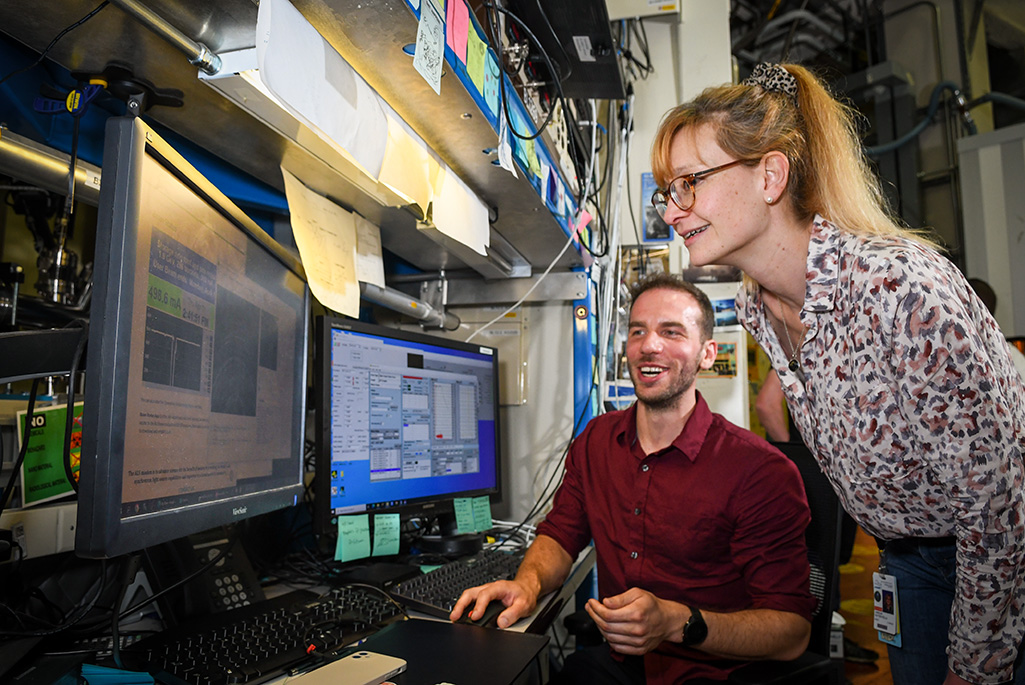
Carolin Sutter-Fella (standing), Staff Scientist, and Tim Kodalle, Postdoctoral Researcher, discuss their research at the Advanced Light Source (ALS). Credit: Thor Swift/Berkeley Lab
Researchers create a more complete picture of what’s happening inside advanced perovskite materials used for solar cell applications.
______________________
Key Takeaways
-Materials known as perovskites show great promise to reduce the costs of solar power but are not yet durable enough to be commercially viable.
-Scientists developed a simplified process to fabricate perovskite solar cell materials with improved durability and efficiency.
-Berkeley Lab researchers used simultaneous characterization techniques to understand why the process worked so well, providing key insights to nudge perovskites closer to commercialization.
______________________
For Michael Saliba and Mahdi Malekshahi, it was one of those moments in science when good experimental results raise more questions. The University of Stuttgart researchers recently developed a new process to make solar cells with perovskites – advanced crystalline materials with potential to revolutionize solar technology. Their cells were very efficient and stable, but there was one catch: they did not have a detailed understanding of why this process worked so well.
Saliba and Malekshahi reached out to researchers at the Molecular Foundry [below], a Department of Energy Office of Science user facility located at Lawrence Berkeley National Laboratory (Berkeley Lab). Fast forward several months, and the Berkeley Lab team has applied a set of techniques to reveal changes in the crystalline structures of perovskite solar cell materials in real time as they were being fabricated with Saliba’s process. The results, published in a recent Advanced Materials paper, provide researchers with a deeper understanding of how to make better perovskite solar cells.
“Material fabrication is often a black box,” said Carolin Sutter-Fella, a Molecular Foundry staff scientist and one of the paper’s corresponding authors. “You can’t see what is happening as the material transforms from its initial building blocks to the final state. We built several capabilities that allow us to watch the formation of perovskite and other printable solar cell materials in fine detail. The insights from this work can help researchers address key barriers to commercializing this promising technology.”
“By continuously taking measurements while depositing the material, we can visually follow how its functional properties evolve,” said Tim Kodalle, a Berkeley Lab postdoctoral researcher at the Molecular Foundry and the study’s lead author. “It’s like watching a video.”
The work was also conducted at the Advanced Light Source [below], a Department of Energy Office of Science User Facility located at Berkeley Lab.
A potential game-changer for solar
Perovskites have numerous advantages over the traditional silicon-based solar panels that dominate the solar industry today. For one, they absorb light much more efficiently. As a result, they can be made 100 times thinner and even printed on surfaces. Because they require less material and lower temperatures to process, they are potentially less expensive to produce. Unlike silicon or other semiconductor panels, perovskites perform well with material impurities.
The elemental composition of perovskites can easily be changed so that they absorb different parts of the sun’s spectrum, which opens exciting opportunities to apply thin perovskite films to silicon panels. The resulting “tandem” panels could be significantly more efficient than today’s panels, potentially enabling cost savings to accelerate the clean energy transition.
Despite these advantages, perovskite solar panels are not commercially viable yet. The main barrier is a lack of stability and durability. Solar panels must be able to last for 20 to 30 years in all kinds of weather. Perovskites attract water and degrade quickly in humid conditions, limiting their long-term durability in the field. Because of their sensitivity to environmental conditions, it’s also difficult to fabricate perovskite cells with consistent quality.
“Two different labs may use the same process to make perovskites with significantly different quality,” said Sutter-Fella. “This makes it hard for researchers to reproduce experiments, compare results, and figure out why some solar cells perform better than others.”
A protective barrier to keep out moisture
One approach to improve durability involves fabricating a perovskite solar cell and then depositing an organic molecule called phenethylammonium chloride or PEACl on its surface. Researchers studying this two-step process have found that the PEACl forms a thin protective barrier that is effective at keeping out moisture.
Saliba’s team at the University of Stuttgart improved this process by integrating perovskite cell fabrication and PEACl deposition into a single step. “Such a simplified process can enable researchers to make cells with more consistent quality,” said Kodalle. “Longer term, the process can potentially reduce the costs and energy consumption of perovskite cell manufacturing.”
Saliba’s lab found that cells made with his process were more durable and efficient than cells made without PEACl. The collaboration with Berkeley Lab provided a more detailed explanation of this observation, characterizing how the perovskite materials evolved structurally as they were made.
Probing perovskites with X-rays, laser beams, and white light
In an approach known as multimodal imaging, the Berkeley Lab team applied three techniques to probe perovskite solar cell materials during fabrication, observing the evolution of their properties as they formed. Two materials were evaluated – one treated with PEACl using the process from Saliba’s lab and the other without PEACl. The results revealed critical differences in the evolution of the two samples.
The first technique, known as grazing incidence wide-angle X-ray scattering, was conducted at the Advanced Light Source, a circular particle accelerator that generates bright X-ray beams. The technique involved illuminating the samples with a beam of X-rays at a shallow angle and measuring the resulting pattern of the X-rays as they scatter off of the atoms in the sample. This information revealed changes in the crystalline structures during the formation of the perovskite layers.
The second technique, called photoluminescence spectroscopy, measured the light emitted by the samples when illuminated by a laser. The changes in the energy of the light emitted by the samples provided insight into their crystal quality. A third technique, conducted at the Molecular Foundry, involved shining white light on the samples and determining the portion of light absorbed by the samples. This technique revealed complementary information to the photoluminescence spectra and X-ray scattering patterns, providing additional insights into the crystal structure of the samples. The researchers then correlated the data streams from the three techniques to produce a detailed understanding of the temporal evolution of the crystalline structure of the samples.
The techniques revealed that the crystals in the PEACl-treated samples grew more slowly and were of higher quality, with a protective PEACl-rich layer forming at their surface. The team believes these findings explain the cells’ improved efficiency and stable operation for over a month.
Perovskite Solar Cell Materials
Berkeley Lab researchers hit perovskite solar cell materials with X-rays as the materials were being fabricated. These videos, based on the scattering of the X-rays, show the structural changes happening in two different perovskite samples. The video on the left shows changes in a sample treated with an organic molecule called PEACl. The video on the right shows changes in a sample without PEACl. The red areas in the left video indicate the formation of a protective layer on the perovskite. (Credit: Tim Kodalle, Berkeley Lab)
Sutter-Fella envisions several possible next research steps. “We can treat perovskites with other molecules and see how they affect durability and efficiency,” she said. “We also need to monitor the cell’s stability over a longer period of operation and under more realistic environmental conditions. The idea would be to understand which material combinations improve the cell’s stability and thus can extend its lifetime.”
This research was supported by the Department of Energy’s Office of Science, Office of Basic Energy Sciences; the German Research Foundation; the European Research Council; and the Helmholtz Association/Forschungszentrum Jülich for the Helmholtz Young Investigator Group FRONTRUNNER.
See the full article here .
Comments are invited and will be appreciated, especially if the reader finds any errors which I can correct.

five-ways-keep-your-child-safe-school-shootings
Please help promote STEM in your local schools.
![]()


Bringing Science Solutions to the World
In the world of science, The Lawrence Berkeley National Laboratory (Berkeley Lab) is synonymous with “excellence.” A number of Nobel prizes are associated with Berkeley Lab. Lab scientists are members of the The National Academy of Sciences, one of the highest honors for a scientist in the United States. A number of our scientists have won the National Medal of Science, our nation’s highest award for lifetime achievement in fields of scientific research. A number of our engineers have been elected to the The National Academy of Engineering, and a number of our scientists have been elected into The Institute of Medicine. In addition, Berkeley Lab has trained thousands of university science and engineering students who are advancing technological innovations across the nation and around the world.
Berkeley Lab is a member of the national laboratory system supported by The DOE through its Office of Science. It is managed by the University of California-Berkeley and is charged with conducting unclassified research across a wide range of scientific disciplines. Located on a 202-acre site in the hills above The University of California-Berkeley campus that offers spectacular views of the San Francisco Bay, Berkeley Lab employs a large number of scientists, engineers and support staff. Technologies developed at Berkeley Lab have generated billions of dollars in revenues, and thousands of jobs. Savings as a result of Berkeley Lab developments in lighting and windows, and other energy-efficient technologies, have also been in the billions of dollars.
Berkeley Lab was founded in 1931 by Ernest Orlando Lawrence, a University of California-Berkeley physicist who won the 1939 Nobel Prize in physics for his invention of the cyclotron, a circular particle accelerator that opened the door to high-energy physics. It was Lawrence’s belief that scientific research is best done through teams of individuals with different fields of expertise, working together. His teamwork concept is a Berkeley Lab legacy that continues today.
History
1931–1941
The laboratory was founded on August 26, 1931, by Ernest Lawrence, as the Radiation Laboratory of the University of California-Berkeley, associated with the Physics Department. It centered physics research around his new instrument, the cyclotron, a type of particle accelerator for which he was awarded the Nobel Prize in Physics in 1939.

LBNL 88 inch cyclotron.

Throughout the 1930s, Lawrence pushed to create larger and larger machines for physics research, courting private philanthropists for funding. He was the first to develop a large team to build big projects to make discoveries in basic research. Eventually these machines grew too large to be held on the university grounds, and in 1940 the lab moved to its current site atop the hill above campus. Part of the team put together during this period includes two other young scientists who went on to establish large laboratories; J. Robert Oppenheimer founded The DOE’s Los Alamos Laboratory, and Robert Wilson founded The DOE’s Fermi National Accelerator Laboratory.
1942–1950
Leslie Groves visited Lawrence’s Radiation Laboratory in late 1942 as he was organizing the Manhattan Project, meeting J. Robert Oppenheimer for the first time. Oppenheimer was tasked with organizing the nuclear bomb development effort and founded today’s DOE Los Alamos National Laboratory to help keep the work secret. At the RadLab, Lawrence and his colleagues developed the technique of electromagnetic enrichment of uranium using their experience with cyclotrons. The “calutrons” (named after the University) became the basic unit of the massive Y-12 facility in Oak Ridge, Tennessee. Lawrence’s lab helped contribute to what have been judged to be the three most valuable technology developments of the war (the atomic bomb, proximity fuse, and radar). The cyclotron, whose construction was stalled during the war, was finished in November 1946. The Manhattan Project shut down two months later.
1951–2018
After the war, the Radiation Laboratory became one of the first laboratories to be incorporated into the Atomic Energy Commission (AEC) (now The Department of Energy . The most highly classified work remained at Los Alamos, but the RadLab remained involved. Edward Teller suggested setting up a second lab similar to Los Alamos to compete with their designs. This led to the creation of an offshoot of the RadLab (now The DOE’s Lawrence Livermore National Laboratory) in 1952. Some of the RadLab’s work was transferred to the new lab, but some classified research continued at Berkeley Lab until the 1970s, when it became a laboratory dedicated only to unclassified scientific research.
Shortly after the death of Lawrence in August 1958, the UC Radiation Laboratory (both branches) was renamed the Lawrence Radiation Laboratory. The Berkeley location became the Lawrence Berkeley Laboratory in 1971, although many continued to call it the RadLab. Gradually, another shortened form came into common usage, LBNL. Its formal name was amended to Ernest Orlando Lawrence Berkeley National Laboratory in 1995, when “National” was added to the names of all DOE labs. “Ernest Orlando” was later dropped to shorten the name. Today, the lab is commonly referred to as “Berkeley Lab”.
The Alvarez Physics Memos are a set of informal working papers of the large group of physicists, engineers, computer programmers, and technicians led by Luis W. Alvarez from the early 1950s until his death in 1988. Over 1700 memos are available on-line, hosted by the Laboratory.
The lab remains owned by the Department of Energy , with management from the University of California-Berkeley. Companies such as Intel were funding the lab’s research into computing chips.
Science mission
From the 1950s through the present, Berkeley Lab has maintained its status as a major international center for physics research, and has also diversified its research program into almost every realm of scientific investigation. Its mission is to solve the most pressing and profound scientific problems facing humanity, conduct basic research for a secure energy future, understand living systems to improve the environment, health, and energy supply, understand matter and energy in the universe, build and safely operate leading scientific facilities for the nation, and train the next generation of scientists and engineers.
The Laboratory’s 20 scientific divisions are organized within six areas of research: Computing Sciences; Physical Sciences; Earth and Environmental Sciences; Biosciences; Energy Sciences; and Energy Technologies. Berkeley Lab has six main science thrusts: advancing integrated fundamental energy science; integrative biological and environmental system science; advanced computing for science impact; discovering the fundamental properties of matter and energy; accelerators for the future; and developing energy technology innovations for a sustainable future. It was Lawrence’s belief that scientific research is best done through teams of individuals with different fields of expertise, working together. His teamwork concept is a Berkeley Lab tradition that continues today.
Berkeley Lab operates five major National User Facilities for the DOE Office of Science:
The Advanced Light Source (ALS) is a synchrotron light source with 41 beam lines providing ultraviolet, soft x-ray, and hard x-ray light to scientific experiments.

The ALS is one of the world’s brightest sources of soft x-rays, which are used to characterize the electronic structure of matter and to reveal microscopic structures with elemental and chemical specificity. About 2,500 scientist-users carry out research at ALS every year. Berkeley Lab is proposing an upgrade of ALS which would increase the coherent flux of soft x-rays by two-three orders of magnitude.
Berkeley Lab Laser Accelerator (BELLA) Center


The DOE Joint Genome Institute supports genomic research in support of the DOE missions in alternative energy, global carbon cycling, and environmental management. The JGI’s partner laboratories are Berkeley Lab, the DOE’s Lawrence Livermore National Laboratory, the DOE’s Oak Ridge National Laboratory (ORNL), the DOE’s Pacific Northwest National Laboratory (PNNL), and the DOE’s HudsonAlpha Institute for Biotechnology . The JGI’s central role is the development of a diversity of large-scale experimental and computational capabilities to link sequence to biological insights relevant to energy and environmental research. A large number of scientist-users take advantage of JGI’s capabilities for their research every year.

The LBNL Molecular Foundry is a multidisciplinary nanoscience research facility. Its seven research facilities focus on Imaging and Manipulation of Nanostructures; Nanofabrication; Theory of Nanostructured Materials; Inorganic Nanostructures; Biological Nanostructures; Organic and Macromolecular Synthesis; and Electron Microscopy. Approximately 700 scientist-users make use of these facilities in their research every year.
The DOE’s NERSC National Energy Research Scientific Computing Center is the scientific computing facility that provides large-scale computing for the DOE’s unclassified research programs. Its current systems provide over 3 billion computational hours annually. NERSC supports 6,000 scientific users from universities, national laboratories, and industry.
DOE’s NERSC National Energy Research Scientific Computing Center at Lawrence Berkeley National Laboratory.


NERSC is a DOE Office of Science User Facility.


The DOE’s Energy Science Network is a high-speed network infrastructure optimized for very large scientific data flows. ESNet provides connectivity for all major DOE sites and facilities, and the network transports roughly 35 petabytes of traffic each month.
Berkeley Lab is the lead partner in the DOE’s Joint Bioenergy Institute (JBEI), located in Emeryville, California. Other partners are the DOE’s Sandia National Laboratory, the University of California (UC) campuses of Berkeley and Davis, the Carnegie Institution for Science , and the DOE’s Lawrence Livermore National Laboratory (LLNL). JBEI’s primary scientific mission is to advance the development of the next generation of biofuels – liquid fuels derived from the solar energy stored in plant biomass. JBEI is one of three new U.S. Department of Energy (DOE) Bioenergy Research Centers (BRCs).
Berkeley Lab has a major role in two DOE Energy Innovation Hubs. The mission of the Joint Center for Artificial Photosynthesis (JCAP) is to find a cost-effective method to produce fuels using only sunlight, water, and carbon dioxide. The lead institution for JCAP is the California Institute of Technology and Berkeley Lab is the second institutional center. The mission of the Joint Center for Energy Storage Research (JCESR) is to create next-generation battery technologies that will transform transportation and the electricity grid. The DOE’s Argonne National Laboratory leads JCESR and Berkeley Lab is a major partner.
