From “physicsworld.com” and [CERN] [La Organización Europea para la Investigación Nuclear][ Organization européenne pour la recherche nucléaire] [Europäische Organization für Kernforschung](CH) : “CERN study reveals organic molecule from trees excels at seeding clouds”

From “physicsworld.com”

And

The European Organization for Nuclear Research [La Organización Europea para la Investigación Nuclear][Organization européenne pour la recherche nucléaire] [Europäische Organization für Kernforschung](CH) [CERN].

Cern New Particle Event

[CERN] [La Organización Europea para la Investigación Nuclear][ Organization européenne pour la recherche nucléaire] [Europäische Organization für Kernforschung](CH)

10.5.23 [Just today in social media.]
Sam Jarman

A family of organic compounds released by trees could play a far greater role in cloud formation than previously thought. That is the conclusion of Lubna Dada at Switzerland’s Paul Scherrer Institute and an international team, who say that their insights could play a crucial role in predicting the future of Earth’s climate.

When trees come under stress, they release organic molecules that react with ozone, nitrate radicals and other compounds in the atmosphere. These reactions create tiny solid particles called ultra-low-volatility organic compounds (ULVOCs).

In some cases, ULVOCs can grow large enough for water droplets to condense on their surfaces, encouraging cloud formation. Clouds have significant effects on Earth’s climate – many of which are poorly understood. Therefore, understanding the influence of ULVOCs cannot be overlooked in global climate models.

The most important molecules involved in ULVOC formation are in three types of hydrocarbon called isoprene, monoterpene and sesquiterpene. To complicate matters, scientists believe climate change is now altering their emission into the atmosphere.

Cloudy at CERN

In the latest study, Dada’s team explored the ability of sesquiterpenes to form ULVOCs using the Cosmics Leaving Outdoor Droplets (CLOUD) chamber at CERN in Geneva.
2
Could there be a link between galactic cosmic rays and cloud formation? An experiment at CERN is using the cleanest box in the world to find out. Credit: CERN.

The “Cosmics Leaving Outdoor Droplets” (CLOUD) experiment uses a special cloud chamber to study the possible link between galactic cosmic rays and cloud formation. Based at the Proton Synchrotron (PS) at CERN, this is the first time a high-energy physics accelerator has been used to study atmospheric and climate science.

CERN Proton Synchrotron

The results should contribute much to our fundamental understanding of aerosols and clouds, and their affect on climate.

There, researchers can simulate different atmospheric conditions that are involved in cloud formation.

“At almost 30 m^3, this sealed climate chamber is the purest of its kind worldwide. It is so pure that it allows us to study sesquiterpenes even at the low concentrations recorded in the atmosphere,” Dada explains.

Starting with a mixture of only isoprene and monoterpene, the team measured how rates of cloud formation changed inside the chamber as the concentration of sesquiterpene was increased. The effect was immediate. Even when sesquiterpene composed just 2% of the mixture inside the CLOUD chamber, its increased yield of ULVOCs had already doubled the cloud formation rate.

As Dada explains, “This can be explained by the fact that a sesquiterpene molecule consists of 15 carbon atoms, while monoterpenes consist of only 10 and isoprenes only five.” With its higher molecular weight, sesquiterpene is far less volatile still than the other two molecules, allowing it to coalesce more readily into solid particles.

The results show that the cloud-forming influence of sesquiterpenes must be included in future global climate models. Dada and colleagues hope that their study will allow climate scientists to make better predictions of how cloud formation and its impact on Earth’s atmosphere will change as the planet continues to heat.

Building on their techniques, the researchers will now aim to gain a broader picture of how the climate has already been impacted by emissions of other artificially created compounds. “Next, we and our CLOUD partners want to investigate what exactly happened during industrialization,” explains team member, Imad El Haddad. “At this time, the natural atmosphere became increasingly mixed with anthropogenic gases such as sulphur dioxide, ammonia and other anthropogenic organic compounds.”

The research is described in Science Advances.

Fig. 1. Example pure biogenic NPF experiment in CLOUD.
3
Here, we show a representative mixture run with all three BVOCs (β-caryophyllene, α-pinene, and isoprene) in three concentration steps, with an injected ratio 1:6:50 (β-caryophyllene, α-pinene, and isoprene), 40 ppbv (parts per billion by volume) O3, T = +5°C, relative humidity (RH) = 40%, and full UV lamp intensity; runs 12 to 14 (see table S1). (A) The combined particle number size distribution measured using a full suite of particle measuring instruments (see the “Particle counters” section in Materials and Methods). (B) Evolution of precursor vapor measured concentrations, α-pinene, β-caryophyllene, and isoprene. The three experimental stages are separated by vertical gray lines. (C) Evolution of formation rate of particles with diameter >1.7 nm (J1.7) and condensation sink (CS). (D) Evolution of oxidation product concentrations measured with NO3-CIMS, total OOMs, extremely low volatility organic compounds (ELVOCs), and ultralow volatility organic compounds (ULVOCs).
Sorry, no links to references.

See the full article here .

Comments are invited and will be appreciated, especially if the reader finds any errors which I can correct. Use “Reply” near the bottom of the post.


five-ways-keep-your-child-safe-school-shootings
Please help promote STEM in your local schools.

http://www.stemedcoalition.org/”>Stem Education Coalition

Meet CERN in a variety of places:

Quantum Diaries
QuantumDiaries

Cern Courier

physicsworld is a publication of the Institute of Physics. The Institute of Physics is a leading scientific society. We are a charitable organization with a worldwide membership of more than 50,000, working together to advance physics education, research and application.

We engage with policymakers and the general public to develop awareness and understanding of the value of physics and, through IOP Publishing, we are world leaders in professional scientific communications.

From The University of Geneva [Université de Genève] (CH) Via “physicsworld.com” : “New photon detector accelerates quantum key distribution”

From The University of Geneva [Université de Genève] (CH)

Via

“physicsworld.com”

4.14.23
Sam Jarman

1
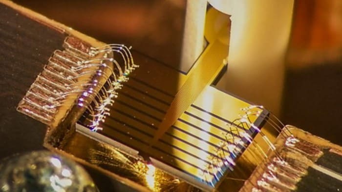
Cool concept: the new single-photon detector makes use of multiple superconducting nanowires. (Courtesy: M Perrenoud and G Resta/UNIGE)

A single-photon detector that could boost the performance of some quantum key distribution (QKD) cryptography systems has been unveiled by Hugo Zbinden and colleagues at the University of Geneva and ID Quantique in Switzerland. The device contains 14 intertwined superconducting nanowires, which share the task of photon detection.

Quantum computers of the future could crack conventional cryptography systems. However, quantum cryptography systems should remain secure from hackers – at least in principle. One such system is quantum key distribution (QKD), which uses the laws of quantum mechanics to ensure that two communicating parties can exchange cryptography keys securely.

QKD involves sending and receiving strings of photons in specific polarization states. If an eavesdropper intercepts this communication, it disrupts the quantum nature of the information thereby alerting the correspondents.

Limited clock rates

While commercial QKD systems are already is use in some specialized applications, more widespread use of the technology is limited by the “clock rate” at which photons can be created, transmitted and detected. “The clock rates of these systems have increased continuously over the past 30 years,” Zbinden says. “But in modern systems, the speed of the detectors and the post-processing become the limiting factor for high secret key rates in QKD.”

These key rates control the speed at which communicating parties can exchange a secure quantum key. Higher key rates enable users to exchange more information – both more securely, and at higher speeds.

Today’s QKD systems use superconducting nanowire single-photon detectors (SNSPDs), which operate a cryogenic temperatures. A small region of the nanowire heats up when it absorbs a photon, switching temporarily from a superconductor to a normal material. This causes an increase in the electrical resistance of the nanowire, which is detected. After the photon is absorbed, the nanowire must cool down before it can detect the next photon – and this recovery time puts a limit on how fast an SNSPD can operate.

Simple yet sophisticated

In its study, Zbinden’s team implemented a simple yet effective fix to this problem. “The novel design of SNSPDs consists of 14 nanowires, which are intertwined in such a way that they are all equally illuminated by the light exiting the optical fibre,” explains Fadri Grünenfelder, Zbinden’s colleague at the University of Geneva. “This increases the chance that there is a wire that still can detect while some others are recovering.”

Another feature of the detector is that each nanowire is shorter than nanowires usually used in SNSPDs – which means that the individual nanowires can cool down faster.

Existing SNSPDs can support key rates of just over 10 Mbps, but the Swiss team has done much better. “The high maximum count rate of the SNSPD, as well as the increased timing resolution, helped to achieve a secret key rate of 64 Mbps over 10 km of optical fibre,” Grünenfelder says. “We could beat the previous record by more than a factor of four.”

Privacy amplification

By detecting photons at this rate, a QKD system could make any necessary error corrections, and carry out privacy amplification (a process which transforms raw key photons into a final secure key, independent of any information which might have leaked to an eavesdropper) – both in real time.

For now, the cryogenic temperatures required for SNSPDs mean the technology is not well suited to everyday applications in QKD. “Other optimizations implemented for pushing key rates to the limit can be implemented in more mainstream, commercial QKD,” Zbinden explains.

However, the researchers still envisage a wide range of possibilities for their ultra-fast, highly efficient SNSPDs: from secure communication between distant spacecraft, to new generations of advanced optical sensors – which could be particularly useful in medical imaging.

The research is described in Nature Photonics.
https://www.nature.com/articles/s41566-023-01168-2
See the science paper for instructive material with images.

See the full article here.

Comments are invited and will be appreciated, especially if the reader finds any errors which I can correct. Use “Reply”.

five-ways-keep-your-child-safe-school-shootings

Please help promote STEM in your local schools.

Stem Education Coalition

The The University of Geneva [Université de Genève] (CH) is a public research university located in Geneva, Switzerland.

It was founded in 1559 by John Calvin as a theological seminary and law school. It remained focused on theology until the 17th century, when it became a center for Enlightenment scholarship. In 1873, it dropped its religious affiliations and became officially secular. Today, the university is the third largest university in Switzerland by number of students. In 2009, the University of Geneva celebrated the 450th anniversary of its founding. Almost 40% of the students come from foreign countries.

The university holds and actively pursues teaching, research, and community service as its primary objectives. In 2016, it was ranked 53rd worldwide by the Shanghai Academic Ranking of World Universities, 89th by the QS World University Rankings, and 131st in the TIMES Higher Education World University Ranking.

UNIGE is a member of the League of European Research Universities (EU) (including academic institutions such as University of Amsterdam [Universiteit van Amsterdam] (NL), University of Cambridge (UK), Ruprecht Karl University of Heidelberg, [Ruprecht-Karls-Universität Heidelberg] (DE), University of Helsinki [ Helsingin yliopisto; Helsingfors universitet] (FI) and University of Milan [Università degli Studi di Milano Statale] (IT)) the Coimbra Group (EU) and the European University Association (EU).

From “physicsworld.com” : “Multiple mirrors magnify atom interferometry”

From “physicsworld.com”

10.20.22
Isabelle Dumé

1
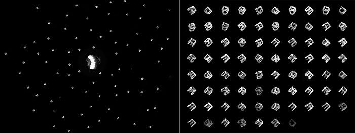
Various views of a 3D-printed object captured by a single camera. (Courtesy: Sanha Cheong/The DOE’s SLAC National Accelerator Laboratory)

A new multiple-mirror imaging technique could greatly improve the performance of atom interferometers, making them more useful in applications ranging from dark matter detection to quality control in manufacturing. By capturing incoming light from many different angles, the new technique enables scientists to collect more light than is possible using conventional imaging set-ups, boosting the system’s sensitivity.

The new technique, which was developed by researchers at The DOE’s SLAC National Accelerator Laboratory, is an example of light-field imaging, which captures not just the intensity of light, but also the direction in which light rays travel. The multiple mirrors redirect the different light views and overlap them onto an imaging sensor. This light field information can then be used to reconstruct a three-dimensional image of an object.

Gravitational searches for dark matter

One possible use for the new technique would be in the Matter-wave Atomic Gradiometer Interferometric Sensor, a 100-metre-long atom interferometer currently being installed at The DOE’s Fermi National Accelerator Laboratory.

2
Matter-wave Atomic Gradiometer Interferometric Sensor (MAGIS-100).

Quantum Science and Technology [below]

“MAGIS-100”, as it is known, will be a new tool in the ongoing search for dark matter – the mysterious substance that is thought to make up 85% of the matter in the universe but is currently only observable through its gravitational influence, which prevents large objects such as galaxies from flying apart as they rotate.

In “MAGIS-100”, researchers will release clouds of strontium atoms in a vacuum tube and then shine laser light on the clouds to image them as they fall within the tube. Each atom acts like a wave and the laser light puts these atomic waves into a superposition of quantum states: one state in which the atom continues down its original path and another in which the light “kicks” it higher up the tube. The two waves then recombine, creating an interference pattern. The relative distance between the pairs of quantum waves is highly sensitive to perturbations and could thus reveal the hidden influence of dark matter.

For this technique to work, however, the laser light needs to be just the right intensity. Too intense, and it will destroy the structure of the atom clouds; not intense enough, and the clouds will be too dim to be picked up by the experiment’s imaging camera (which sits outside the chamber that holds the atoms). One solution to this problem would be to use a camera with a wider aperture, but this would create a narrow depth of field in which only a small part of the image is in focus.

Capturing more light

In the new work, the team led by Murtaza Safdari of Stanford University overcame this problem by reflecting light traveling away from the cloud back into the camera lens. The camera can then gather not just more light, but also more views of an object from different angles, each of which shows up on the image as a distinct spot on a black background. A collection of such distinct images can be used to reconstruct a 3D model of the atom cloud.

“Conventional imaging captures only as much light as the lens aperture can accept, and it necessarily loses directional information since it integrates light over the aperture of the lens,” Safdari tells Physics World. “Conventional spatially multiplexed light field imaging is also hampered by the limited lens aperture. Our system is able to benefit from the 3D information capturing ability of spatially multiplexed systems, while also capturing more light than the lens’ aperture would conventionally allow.”

Safdari adds that while the system would directly benefit imaging in atom interferometer experiments like “MAGIS-100”, it could also have other applications, such as parts inspection on production lines and particle tracking. He and his colleagues are now adapting their design concept to take images of atom clouds in a magneto-optical trap at Stanford, while in the longer term they would like to develop an in-vacuum version of the system to install at “MAGIS-100”.

The present work is detailed in the Journal of Instrumentation.
See this science paper for detailed material with images.

Science paper:
Quantum Science and Technology

See the full article here .


five-ways-keep-your-child-safe-school-shootings
Please help promote STEM in your local schools.

http://www.stemedcoalition.org/”>Stem Education Coalition

physicsworld is a publication of the Institute of Physics. The Institute of Physics is a leading scientific society. We are a charitable organization with a worldwide membership of more than 50,000, working together to advance physics education, research and application.

We engage with policymakers and the general public to develop awareness and understanding of the value of physics and, through IOP Publishing, we are world leaders in professional scientific communications.

From “physicsworld.com” : “Self-assembling microlaser adapts to its environment”

From “physicsworld.com”

7.29.22 [Just today in social media.]
Sam Jarman

1
Life-like laser: Titanium dioxide microparticles clustering around a Janus particle. The dashed line delineates the lasing area, and the pink/yellow lines show the 275 s-long tracks of several microparticles. (Courtesy: Imperial College London)

Physicists in the UK have designed a self-assembling photonic system which can actively adapt the laser beams it produces in response to changing illumination. The team, led by Riccardo Sapienza at Imperial College London and Giorgio Volpe at University College London, based their design around a system of suspended microparticles which formed dense clusters when the mixture was illuminated.

Many systems in nature can harness the energy in their surrounding environments to form coordinated structures and patterns within groups of individual elements. These range from schools of fish, which dynamically change their shape to evade predators, to the folding of proteins in response to bodily functions, such as muscle contraction.

An extensive field of research is now dedicated to emulating this self-organization in artificial materials, which can adapt and reconfigure themselves in response to their changing surroundings. In this latest research, reported in Nature Physics [below], Sapienza and Volpe’s team aimed to reproduce the effect in a laser device, which changes the light it produces as its environment is altered.

To achieve this, the researchers exploited a unique class of materials named colloids, in which particles are dispersed throughout a liquid. Since these particles can be easily synthesized with sizes comparable to the wavelengths of visible light, colloids are already widely used as the building blocks of advanced photonic devices – including lasers.

When their particles are suspended in solutions of laser dyes, these mixtures can scatter and amplify the light trapped within them, producing laser beams through optical pumping with another high-energy laser. So far, however, these designs have largely involved static colloids, whose particles can’t reconfigure themselves as their surroundings change.

In their experiment, Sapienza, Volpe and colleagues introduced a more advanced colloid mixture, in which titanium dioxide (TiO2) particles were evenly suspended in an ethanol solution of laser dye also containing Janus particles (which have two distinct sides with different physical properties). One half of the spherical surfaces of the Janus particles was left bare, while the other was coated with a thin layer of carbon, altering its thermal properties.

This meant that when the Janus particles were illuminated with a 632.8 nm HeNe laser, they generated a molecular-scale temperature gradient in the liquid surrounding them. This caused the TiO2 particles in the colloid to cluster themselves around the hot Janus particle and form an optical cavity. Once the illumination ended, the Janus particle cools and the particles disperse back to their original, uniform arrangements.

This unique behaviour allowed Sapienza and Volpe’s team to carefully control the sizes and densities of their TiO2clusters. Through optical pumping, they showed that sufficiently dense clusters could produce an intense laser, spanning a narrow range of visible wavelengths. The process was also completely reversible, with the laser dimming and broadening once illumination was removed.

In demonstrating a laser system that can actively respond to changes in illumination, the researchers hope their results could inspire a new generation of self-assembling photonic materials: suitable for applications as wide-ranging as sensing, light-based computing and smart displays.

Science paper:
Nature Physics

See the full article here.


five-ways-keep-your-child-safe-school-shootings
Please help promote STEM in your local schools.

http://www.stemedcoalition.org/”>Stem Education Coalition

physicsworld is a publication of the Institute of Physics. The Institute of Physics is a leading scientific society. We are a charitable organization with a worldwide membership of more than 50,000, working together to advance physics education, research and application.

We engage with policymakers and the general public to develop awareness and understanding of the value of physics and, through IOP Publishing, we are world leaders in professional scientific communications.

From “physicsworld.com” : “Polarization switch makes ultrafast photonic computer”

From “physicsworld.com”

7.22.22 [Just today in social media.]
Isabelle Dumé

1
Hybrid nanowires that can selectively switch the devices depending on polarization. Courtesy: June Sang Lee, Department of Materials, University of Oxford.

Materials that switch from one phase to another when illuminated by light with different polarizations could form a platform for ultrafast photonic computing and information storage, say researchers at the University of Oxford, UK. The materials take the form of structures known as hybridized-active-dielectric nanowires, and the researchers say they could become part of a multiwire system for parallelized data storage, communications and computing.

Because different wavelengths of light do not interact with each other fibre optic cables can transmit light at multiple wavelengths, carrying streams of data in parallel. Different polarizations of light also do not interact with each other, so in principle each polarization could similarly be employed as an independent information channel. This would allow more information to be stored, dramatically increasing information density.

But while wavelength-selective systems for transmitting data are common, polarization-selective alternatives have not been widely explored, explains study lead author June Sang Lee. “Our work shows the first prototype of programmable device using polarizations and it maximizes the density of information processing,” he tells Physics World. Photonics has a huge advantage over electronics in this respect, he adds, since light travels faster than electrons and functions over large bandwidths. “Indeed, the computing density of our device is several orders of magnitude larger than that of conventional electronics.”

Functional nanowires

The new photonic computing processor consists of functional nanowires made of a phase-change material, Ge2Sb2Te5(GST), and silicon, which acts as a dielectric. The researchers connected the nanowires, each of which is 15 µm long and 180 nm wide, to two metal electrodes. This set-up allowed them to measure the electric current through the GST while they illuminated it with light pulses from a 638-nm-wavelength laser.

When illuminated with this light, the phase of the active material switches reversibly from a highly resistive (amorphous) state to a conductive (crystalline) one. The researchers can therefore use the polarization of the incoming light to tune the absorption of light by the active layer.

“The interesting point is that each nanowire shows a selective switching response to a specific polarization direction of optical pulses,” Lee says. “Using this concept, we have implemented the photonic computing processor with multiple nanowires so that multiple polarizations of light can independently interact with different nanowires and perform parallel computing.”

The researchers describe the study, which is published in Science Advances [below], as early-stage work towards a large-scale photonic computing device. “We would like to scale up such functionality by changing the device configuration or by using integrated photonic circuits,” Lee reveals. “We would also like to further investigate other nanostructures that can exploit the properties of polarization.”

Science paper:
Science Advances

See the full article here.


five-ways-keep-your-child-safe-school-shootings
Please help promote STEM in your local schools.

http://www.stemedcoalition.org/”>Stem Education Coalition

physicsworld is a publication of the Institute of Physics. The Institute of Physics is a leading scientific society. We are a charitable organization with a worldwide membership of more than 50,000, working together to advance physics education, research and application.

We engage with policymakers and the general public to develop awareness and understanding of the value of physics and, through IOP Publishing, we are world leaders in professional scientific communications.

From “physicsworld.com” : “X-ray microscopy sharpens up”

From “physicsworld.com”

7.19.22 [Just today in social media.]
Isabelle Dumé

1
Constructing a sharp image of precisely arranged concentric layers to image two semiconductor nanowires. (Courtesy: Markus Osterhoff)

A new algorithm that compensates for deficiencies in X-ray lenses could make images from X-ray microscopes much sharper and higher in quality than ever before, say researchers at the University of Göttingen, Germany. Preliminary tests carried out at the German Electron Synchrotron (DESY) in Hamburg showed that the algorithm makes it possible to achieve sub-10-nm resolution and quantitative phase contrast even with highly imperfect optics.

Standard X-ray microscopes are non-destructive imaging tools capable of resolving details down to the 10 nm level at ultrafast speeds. There are three main techniques. The first is transmission X-ray microscopy (TXM), which was developed in the 1970s and which uses Fresnel zone plates (FZPs) as objective lenses to directly image and magnify the structure of a sample. The second is coherent diffractive imaging, which was developed to sidestep the problems associated with imperfect FZP lenses by replacing lens-based image formation with an iterative phase retrieval algorithm. The third technique, full-field X-ray microscopy, is based on inline holography and has both high resolution and an adjustable field of view, making it very good for imaging biological samples with weak contrast.

Combining three techniques

In the new work, researchers led by Jakob Soltau, Markus Osterhoff and Tim Salditt from Göttingen’s Institute for X-ray Physics showed that by combining aspects of all three techniques, it is possible to achieve much higher image quality and sharpness. To do this, they used a multilayer zone plate (MZP) as an objective lens to achieve high image resolution, coupled with a quantitative iterative phase retrieval scheme to reconstruct how X-rays transmit through the sample.

The MZP lens is made of finely structured layers a few atomic layers thick deposited from concentric rings on a nanowire. The researchers placed it at an adjustable distance between the sample being imaged and an X-ray camera in the extremely bright and focused X-ray beam at DESY. The signals that hit the camera provided information about the structure of the sample – even if it absorbed little or no X-ray radiation. “All that remained was to find a suitable algorithm to decode the information and reconstruct it into a sharp image,” Soltau and colleagues explain. “For this solution to work, it was crucial to precisely measure the lens itself, which was far from perfect, and to completely dispense with the assumption that it could be ideal.”

“It was only through the combination of lenses and numerical image reconstruction that we could achieve the high image quality,” Soltau continues. “To this end, we used the so-called MZP transfer function, which allows us to do away with perfectly aligned, aberration- and distortion-free optics, among other constraints.”

The researchers have dubbed their technique “reporter-based imaging” because, unlike conventional approaches that make use of an objective lens to acquire a sharper image of the sample, they use the MZP to “report” the light field behind the sample, rather than trying to obtain a sharp image in the plane of the detector.

Full details of the research are published in Physical Review Letters.

See the full article here .


five-ways-keep-your-child-safe-school-shootings
Please help promote STEM in your local schools.

http://www.stemedcoalition.org/”>Stem Education Coalition

physicsworld is a publication of the Institute of Physics. The Institute of Physics is a leading scientific society. We are a charitable organization with a worldwide membership of more than 50,000, working together to advance physics education, research and application.

We engage with policymakers and the general public to develop awareness and understanding of the value of physics and, through IOP Publishing, we are world leaders in professional scientific communications.
From “physicsworld.com” : “Near-unipolar laser pulses could control qubits”

From “physicsworld.com”

7.1.22 [Just today in social media.]
Isabelle Dumé

1
Effectively unipolar light wave. (Courtesy: Christian Meineke, Huber Lab, University of Regensburg)

Physicists have created a light wave that is effectively unipolar meaning it behaves as though it is solely a positive field pulse rather than the usual positive–negative oscillation found in electromagnetic waves. The positive pulse has a sharp peak and high amplitude and is powerful enough to switch or move electronic states, meaning that it could be used to manipulate quantum information and perhaps accelerate conventional computing as well.

Electromagnetic waves, and in particular light pulses, can be used to switch, characterize, and control electronic quantum states with incredible accuracy, explain team leaders Mackillo Kira and Rupert Huber of the University of Michigan in the US and the University of Regensburg in Germany. However, the shape of such pulses is fundamentally restricted to a combination of positive and negative oscillations that sum to zero. As a result, the positive cycle may move charge carriers (electrons or holes), but then the negative cycle pulls them back to square one.

Positive peak is strong enough to switch or move electronic states.

An ideal quantum-electronic switch pulse would be so highly asymmetrical as to be completely unidirectional – in other words, it would contain only a positive (or negative) half-cycle of field oscillation. Under these conditions, such a pulse could flip a quantum state, such as a quantum bit, in minimum time (a half cycle) and with maximum efficiency (no back-and-forth oscillations).

This is fundamentally impossible for freely-propagating waves, but Kira, Huber and colleagues found a way to create the “next best thing” in the form of a quasi-unipolar wave consisting of a very short, high-amplitude positive peak sandwiched between two long, low-amplitude negative peaks. “The positive peak is strong enough to switch or move electronic states,” Kira and Huber explain, “while the negative peaks are too small to have much of an effect.”

In their work, the researchers started with a newly developed stack of nanofilms made of different semiconductor materials, such as indium gallium arsenide (InGaAs) that was grown epitaxially on gallium arsenide antimonide (GaAsSb). Each of the nanofilms is only a few atoms thick, and at the interface between them, ultrashort laser pulses can excite electrons mainly in the InGaAs film. The holes left behind by the excited electrons remain in the GaAsSb film, creating a charge separation.

Effective half-cycle light pulses

“We then made use of our quantum-theoretical breakthrough in exploiting the electrostatic attraction between the oppositely charged electrons and holes to pull them back together in a precisely controlled way,” Kira tells Physics World. “The fast charging and slower charge oscillations combined emitted the unipolar wave that we tailored as effective half-cycle light pulses in the far-infrared and terahertz part of the electromagnetic spectrum.”

Huber describes the resulting terahertz emission as “stunningly unipolar”, with the single positive half-cycle peaking about four times higher than the two negative peaks. While researchers have been working for a long time on producing light pulses with fewer and fewer oscillation cycles, the possibility of generating terahertz pulses so short that they effectively comprise less than a single half-oscillation cycle was, he adds, “beyond our bold dreams”.

Kira and Huber say that these unipolar terahertz fields could be a powerful tool for controlling novel quantum materials on time scales that are comparable to microscopic electronic motion. The researchers suggest that the fields could also serve as superior, well-defined “clockworks” for next-generation ultrafast electronics. Finally, the new emitters are, they claim, “perfectly adapted” to operate in combination with industry-grade high-power solid-state lasers and could thus form “an extremely scalable platform for applications in both fundamental science and industry”.

The researchers, who report their work in Light: Science & Applications [below], say they have begun to use these pulses to explore new platforms for quantum information processing. “Other applications include coupling these pulses into a scanning tunnelling microscope, which allows us to speed up atomic-resolution microscopy to few-femtosecond time scales (1 fs = 10^-15 s), and thus capture the real-space and -time motion of electrons in actual ultraslow-motion microscopic videos,” they explain.

Science paper:
Light: Science & Applications

See the full article here .


five-ways-keep-your-child-safe-school-shootings
Please help promote STEM in your local schools.

http://www.stemedcoalition.org/”>Stem Education Coalition

physicsworld is a publication of the Institute of Physics. The Institute of Physics is a leading scientific society. We are a charitable organization with a worldwide membership of more than 50,000, working together to advance physics education, research and application.

We engage with policymakers and the general public to develop awareness and understanding of the value of physics and, through IOP Publishing, we are world leaders in professional scientific communications.

From “physicsworld.com” : “Quasiparticle camera images superfluid vortices in helium-3”

From “physicsworld.com”

1
On reflection Diagram showing how some particles are blocked by superfluid vortices by the process of Andreev reflection. (Courtesy: MT Noble et al/Phys. Rev. B)

Physicists in the UK have created a camera that can image the complex tangles of vortices that form inside a helium-3 superfluid. Developed by Theo Noble and colleagues at Lancaster University, the approach could help researchers to better understand the behaviour of quantum fluids.

When cooled to temperatures just above absolute zero, liquid helium-3 becomes a superfluid, which below a certain critical velocity, can flow without any loss of kinetic energy. The effect arises because at very low temperatures atoms of helium-3 – which are fermions – can form Cooper pairs. These pairs are bosons, which means that helium-3 can become a superfluid.

Physicists are fascinated by the dynamics of superfluid helium-3 at high flow velocities. Here, thermal fluctuations break Cooper pairs to create quasiparticles that propagate through the superfluid. These structures cannot exist within a certain energy range, which can prevent them from entering certain regions of a superfluid. As quasiparticles approach these regions, they will trap a partner to form a Cooper pair, leaving behind a quasiparticle called a hole, which propagates in the opposite direction – a process called “Andreev reflection”.

Tangled vortices

This process can be triggered by the quantized vortices that form around obstacles to the flow of a superfluid. In liquid helium-3, these vortices can exist as a disorderly tangle of strings just tens of nanometres thick and can shift the forbidden range of quasiparticles in the fluid by a certain amount – which varies with distance from the vortex.

A variety of techniques have been used to probe these structures: including measuring the magnetic fields surrounding helium-3 nuclei and passing sound waves through the fluid. Yet so far, physicists have struggled to image these tangles directly without the use of invasive techniques, such as artificial tracer particles.

The Lancaster team used a partially closed box within their superfluid to create quasiparticles using a vibrating curved wire. Some of the quasiparticles could move into the rest of the superfluid via a small hole in the box – thus creating a beam of quasiparticles. Upon leaving the box, the beam encounters another vibrating wire that creates a “turbulent tangle” of vortices. Quasiparticles that pass through the tangle are then detected using a 5×5 array of quartz tuning fork resonators.

New discoveries

This allowed the team to produce a series of pixelated images revealing the shadows of vortices, where the quasiparticle beam had been blocked by Andreev reflection. Using this method, the team has already made new discoveries about the properties of superfluid helium-3. For example, they observed many more vortices appeared on the inner edge of the curved wire than its outer edge, despite flow velocities being roughly the same on each side.

The team intends to study these effects in more detail through further improvements to the set-up: including larger pixel arrays, and higher operation speeds to enable video recordings. If achieved, these improvements could allow researchers to mimic a wide variety of complex, large-scale flow patterns in quantum fluids: including sudden accelerations in the rotations of neutron stars; and the break-up of Cooper pairs by incoming cosmic rays, or even by as-yet undiscovered dark matter particles.

The research is described in Physical Review B.

See the full article here .


five-ways-keep-your-child-safe-school-shootings
Please help promote STEM in your local schools.

http://www.stemedcoalition.org/”>Stem Education Coalition

physicsworld is a publication of the Institute of Physics. The Institute of Physics is a leading scientific society. We are a charitable organisation with a worldwide membership of more than 50,000, working together to advance physics education, research and application.

We engage with policymakers and the general public to develop awareness and understanding of the value of physics and, through IOP Publishing, we are world leaders in professional scientific communications.
From “physicsworld.com” : “Flexible organic LED produces ‘romantic’ candle-like light”

From “physicsworld.com”

29 Jun 2022
Isabelle Dumé

1
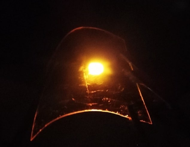
A bendable organic LED with a natural mica backing releases a strong, candlelight-like glow. (Courtesy: Andy Chen and Ambrose Chen)

A new bendable organic light-emitting diode (OLED) that produces warm, candle-like light with hardly any emissions at blue wavelengths might find a place in flexible lighting and smart displays that can be used at night without disrupting the body’s biological clock. The device, which is an improved version of one developed recently by a team of researchers from National Tsing Hua University in Taiwan, is made from a light-emitting layer on a mica substrate that is completely free of plastic.

Jwo-Huei Jou and Ying-Hao Chu of the National Tsing Hua University’s Department of Materials Science and Engineering and colleagues recently patented OLEDS that produce warm, white light. However, these earlier devices still emit some unwanted blue light, which decreases the production of the “sleep hormone” melatonin and can therefore disrupt sleeping patterns. A further issue is that these OLEDs were made of solid materials and were therefore not flexible.

Mica, a natural layered mineral

One way to make OLEDs flexible is to paste them onto a plastic backing, but most plastics cannot be bent repeatedly – a prerequisite for real-world flexible applications. Jou, Chu and colleagues therefore decided to investigate backings made from mica, a natural layered mineral that can be cleaved into bendable, transparent sheets.

The researchers began by depositing a clear indium tin oxide (ITO) film onto a mica sheet as the LED’s anode. They then mixed a luminescent material, N,N’-dicarbazole-1,1’-biphenyl, with red and yellow phosphorescent dyes to fabricate the device’s light-emitting layer. Next, they sandwiched this layer between electrically conductive solutions with the anode on one side and an aluminium layer in the other to create a flexible OLED.

Tests showed that when coated with a transparent conductor, the mica substrate is robust to bending curvatures of 1/5 mm^-1 – a record high – and 50 000 bending cycles at a 7.5 mm bending radius. The OLED is also highly resistant to moisture and oxygen and has a lifetime that is 83% of similar devices on glass.

“Romantic” light

The new device emits bright, warm light upon the application of a constant current. This light contains even less blue-wavelength light than natural candlelight, Jou and Chu report, meaning that the exposure limit for humans is 47 000 seconds compared to just 320 s for a cold-white counterpart, according to the team’s calculations. This means that a person exposed to the OLED for 1.5 hours would see their melatonin production suppressed by about 1.6%, compared to 29% for a cold-white compact fluorescent lamp over the same period.

“We have fabricated an OLED emitting a psychologically-warm but physically-cool, scorching-free romantic candle-like light on a bendable mica substrate using our patented candlelight OLED technology,” Jou tells Physics World. “This technology could provide designers and artists with more freedom in designing variable lighting systems that fit into different spaces, thanks to their flexibility.”

The researchers now hope to make their OLEDs completely transparent. “When lit, these candlelight OLEDs could then be seen from both sides,” Chu says.

The present work is detailed in ACS Applied Electronic Materials.

See the full article here .


five-ways-keep-your-child-safe-school-shootings
Please help promote STEM in your local schools.

http://www.stemedcoalition.org/”>Stem Education Coalition

physicsworld is a publication of the Institute of Physics. The Institute of Physics is a leading scientific society. We are a charitable organisation with a worldwide membership of more than 50,000, working together to advance physics education, research and application.

We engage with policymakers and the general public to develop awareness and understanding of the value of physics and, through IOP Publishing, we are world leaders in professional scientific communications.

From “physicsworld.com” : “Adapting a Surface Microscopy Tool for Quantum Studies”

From “physicsworld.com”

Tyler Harvey | Lawrence Berkeley National Laboratory

Scanning electron microscopes using laser-engineered electron quantum states enter the quantum optics ring.

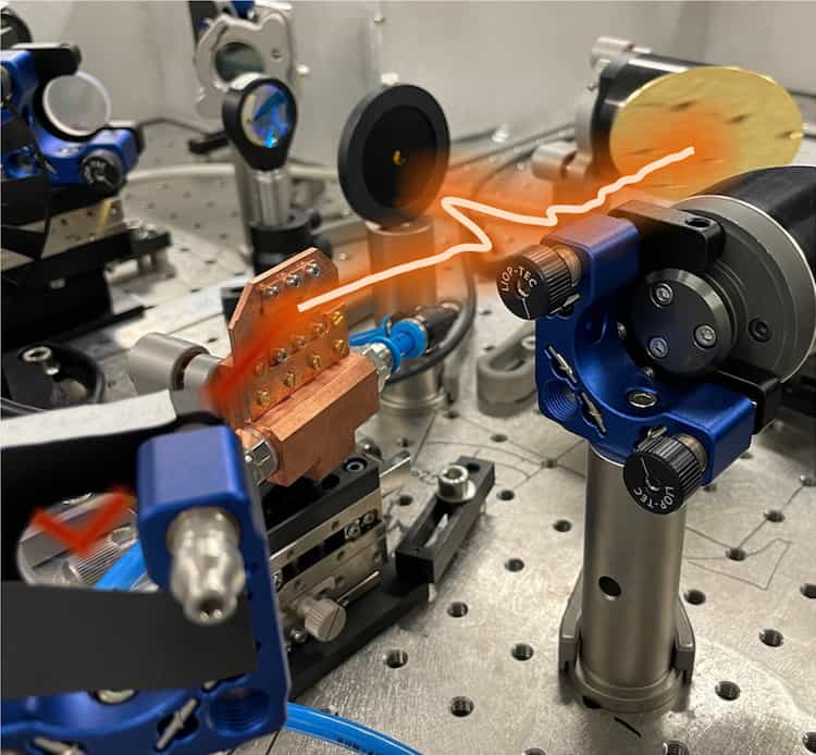
Custom-designed scanning transmission electron microscope at Cornell University by David Muller/Cornell University

1
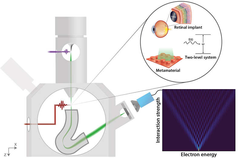
An ultraviolet laser pulse (purple) triggers photoemission of an electron pulse (green) from the scanning electron microscope’s electron source. These electrons are focused onto the specimen—for this instrument, possibilities include just-fabricated metamaterials, in situ retinal implants, or two-level quantum systems such as a quantum dot—where they interact with the optical field of a second infrared laser pulse (red). This interaction can prepare electrons into a superposition of energy states separated exactly by the infrared photon energy, as recorded by a spectrometer. The lower right inset shows electron energy spectra with increasing interaction strength along the vertical axis.

Often, the best way to understand the structure and behavior of a material is to examine it under a microscope. To reveal features on a scale smaller than the wavelength of visible light—about 1/100th the width of human hair—electrons are often the right tool for the job. Researchers have used transmission electron microscopes (TEMs) to image the motion of single atoms and the structure of SARS-CoV-2, the virus that causes COVID-19. Scanning electron microscopes (SEMs) are smaller and less expensive instruments that operate at lower energies and can image the surface of a material in its original form. SEMs can map the elemental composition of rocks right out of the ground, identify single nanoscale defects in hundreds of thousands of computer chips, and even print 3D microscale prototypes. In addition to their day jobs as imaging tools, TEMs have recently taken up a side hustle as a workbench for quantum-mechanics experiments. Now, researchers from the University of Erlangen-Nuremberg in Germany have built an SEM with quantum credentials [1*].

One avenue for quantum experiments in an electron microscope involves simultaneously shooting electrons and a laser beam at a material so that electrons inelastically scatter with the laser photons[2]. Electrons cannot absorb or emit a photon in free space as doing so would violate conservation of energy and momentum. However, a material offers just the kick needed to conserve both energy and momentum so an electron can exchange photons with the laser field [3]. An electron energy spectrum recorded after many electrons have participated in this inelastic electron-light interaction shows a range of evenly spaced peaks separated by the photon energy of the laser (Fig. 1). Because the laser field essentially behaves in a classical way, electrons emerge from the interaction in a controllable, nearly pure quantum state—in other words, the laser can be used to shape the electron state. And the electron state is special: a train of attosecond electron pulses forms with a period equal to the optical cycle of the laser [4]. These pulses could probe the fastest dynamics in materials [4]. A second interaction can then reverse the first one—and restore the original electron state—through destructive interference [5]. Inelastic electron-light scattering (IELS) can prepare electrons into an engineered quantum state for the purposes of imaging or studying quantum interactions.

Between the potential to directly image the fastest material dynamics at atomic scales and the ability to engineer electron states using a laser, excitement has grown recently about IELS. For example, on the basic quantum side, researchers have used IELS to swirl electrons into a vortex state [6]. On the applied side, imaging with IELS is called photon-induced near-field electron microscopy (PINEM). PINEM has imaged the optical properties of systems such as surface plasmons and nanoparticles [2], proteins and cells [7], and even chiral nanostructures [8]. The SEM built by the University of Erlangen-Nuremberg team is capable of both performing quantum-mechanics experiments with electrons and imaging challenging specimens with PINEM.

PINEM was first developed in a TEM, an area where electron spectrometers are commercially available. Measuring the quantized change in electron energy that occurs when electrons interact with the laser field is relatively easy. The tricky part is achieving a high laser field: femtosecond or picosecond electron and laser pulses are typically used for the combination of high peak fields and low average power [3]. For multiple IELS interactions, which are necessary for more elaborate engineering of the electron state, the millimeter-scale gap where specimens sit in a TEM limits the tool’s versatility, whereas SEMs have a large specimen chamber that the operator can reach into with both hands, making experiments with multiple IELS interactions easier. The lower available electron energies of an SEM may also prove useful for a range of specimens; there may be resonances or other maxima in the electron-light scattering depending on geometry [7, 8], or the PINEM signal may be too weak at TEM energies to effectively image the specimen but sufficiently strong at lower energies [3, 8]. Additionally, the lower cost of SEMs makes them more accessible to new groups wanting to do IELS or PINEM experiments.

The instrument that the team developed makes PINEM possible in an SEM. They modified an electron source to produce picosecond electron pulses when struck by a laser pulse, added a path for a femtosecond pulsed laser to excite the specimen, and built an electron spectrometer for their SEM. Each of these steps is a significant project, but the group really triumphed by tying all the elements together: they characterized the instrument and probed a tungsten needle with PINEM. The measured electron spectra matched their simulations remarkably well, which suggests that they have an excellent understanding of the instrument they designed.

It will be exciting to see what experiments follow with this instrument. The ample space in an SEM chamber allowed this group to place a lens with a short focal length very close to the specimen. Doing so may allow them to produce a high laser field on the specimen. The tightly focused laser spot leads to a higher PINEM signal without increasing the average temperature of the specimen, making specimens with a weaker optical response more practical to image. PINEM in an SEM could also shed new light on larger specimens, such as a 3D metamaterial device, that do not fit into a TEM. This new microscope may help motivate the increasing availability of commercial SEM electron spectrometers, which would make building future PINEM-SEMs far easier. The wide-open specimen chamber and the uniquely low energy range give this instrument the ability to push the limits of PINEM imaging and of quantum experiments with electrons.

*References

R. Shiloh et al., “Quantum-coherent light-electron interaction in a scanning electron microscope,” Phys. Rev. Lett. 128, 235301 (2022).
B. Barwick et al., “Photon-induced near-field electron microscopy,” Nature 462, 902 (2009).
S. T. Park et al., “Photon-induced near-field electron microscopy (PINEM): theoretical and experimental,” New J. Phys. 12, 123028 (2010).
K. E. Priebe et al., “Attosecond electron pulse trains and quantum state reconstruction in ultrafast transmission electron microscopy,” Nat. Photon. 11, 793 (2017).
K. E. Echternkamp et al., “Ramsey-type phase control of free-electron beams,” Nat. Phys. 12, 1000 (2016).
G. M. Vanacore et al., “Ultrafast generation and control of an electron vortex beam via chiral plasmonic near fields,” Nat. Mater. 18, 573 (2019).
T. R. Harvey et al., “Probing chirality with inelastic electron-light scattering,” Nano Lett. 20, 4377 (2020).
N. Talebi, “Strong interaction of slow electrons with near-field light visited from first principles,” Phys. Rev. Lett. 125, 080401 (2020).

See the full article here .


five-ways-keep-your-child-safe-school-shootings
Please help promote STEM in your local schools.

http://www.stemedcoalition.org/”>Stem Education Coalition

physicsworld is a publication of the Institute of Physics. The Institute of Physics is a leading scientific society. We are a charitable organisation with a worldwide membership of more than 50,000, working together to advance physics education, research and application.

We engage with policymakers and the general public to develop awareness and understanding of the value of physics and, through IOP Publishing, we are world leaders in professional scientific communications.