
From The DOE’s Lawrence Berkeley National Laboratory
6.11.24
Theresa Duque
tnduque@lbl.gov
Researchers demonstrate a programmable approach to fabricating optical qubits in silicon for large-scale manufacturing.
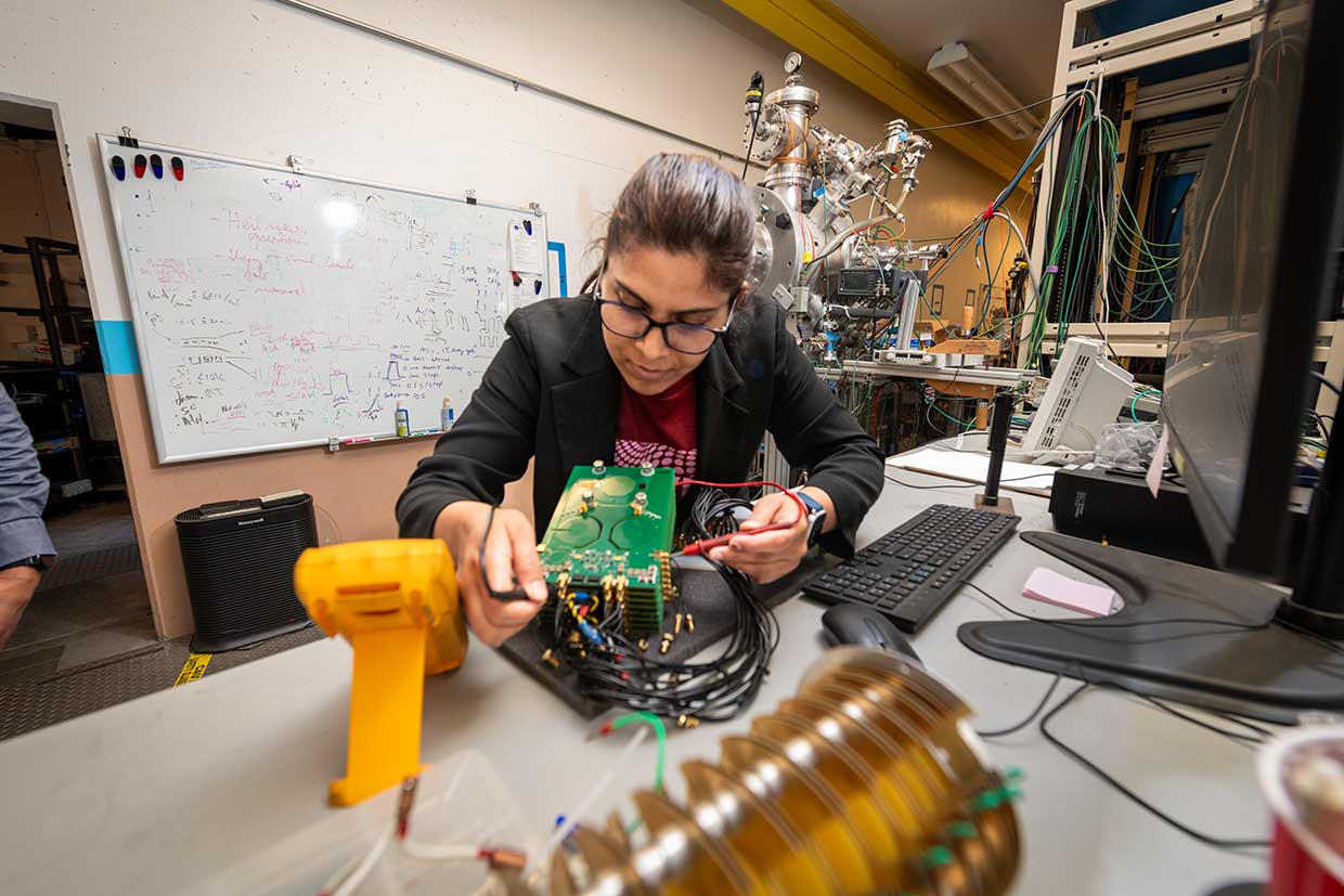
Kaushalya Jhuria in the lab testing the electronics that are part of the experimental setup used for making qubits in silicon. Credit: Thor Swift/Berkeley Lab
Quantum computers have the potential to solve complex problems in human health, drug discovery, and artificial intelligence millions of times faster than some of the world’s fastest supercomputers.


A network of quantum computers could advance these discoveries even faster. But before that can happen, the computer industry will need a reliable way to string together billions of qubits – or quantum bits – with atomic precision.
_______________________
Key Takeaways
-Berkeley Lab researchers have reported a major advancement that could bring us closer to a scalable quantum computer.
-Using a femtosecond laser during experiments which explore the role of hydrogen in qubit formation, the researchers developed a method that programs the formation of telecom-band optical qubits in silicon for large-scale manufacturing.
-The technique could enable scalable quantum computers of the future by building on current silicon-based computing infrastructure.
_______________________
Connecting qubits, however, has been challenging for the research community. Some methods form qubits by placing an entire silicon wafer in a rapid annealing oven at very high temperatures. With these methods, qubits randomly form from defects (also known as color centers or quantum emitters) in silicon’s crystal lattice. And without knowing exactly where qubits are located in a material, a quantum computer of connected qubits will be difficult to realize.
But now, getting qubits to connect may soon be possible. A research team led by Lawrence Berkeley National Laboratory (Berkeley Lab) says that they are the first to use a femtosecond laser to create and “annihilate” qubits on demand, and with precision, by doping silicon with hydrogen.
The advance could enable quantum computers that use programmable optical qubits or “spin-photon qubits” to connect quantum nodes across a remote network. It could also advance a quantum internet that is not only more secure but could also transmit more data than current optical-fiber information technologies.
“To make a scalable quantum architecture or network, we need qubits that can reliably form on-demand, at desired locations, so that we know where the qubit is located in a material. And that’s why our approach is critical,” said Kaushalya Jhuria, a postdoctoral scholar in Berkeley Lab’s Accelerator Technology & Applied Physics (ATAP) Division. She is the first author on a new study that describes the technique in the journal Nature Communications. “Because once we know where a specific qubit is sitting, we can determine how to connect this qubit with other components in the system and make a quantum network.”
“This could carve out a potential new pathway for industry to overcome challenges in qubit fabrication and quality control,” said principal investigator Thomas Schenkel, head of the Fusion Science & Ion Beam Technology Program in Berkeley Lab’s ATAP Division. His group will host the first cohort of students from the University of Hawai’i in June as part of a DOE Fusion Energy Sciences-funded RENEW project on workforce development where students will be immersed in color center/qubit science and technology.
The new method uses a gas environment to form programmable defects called “color centers” in silicon. These color centers are candidates for special telecommunications qubits or “spin photon qubits.” The method also uses an ultrafast femtosecond laser to anneal silicon with pinpoint precision where those qubits should precisely form. A femtosecond laser delivers very short pulses of energy within a quadrillionth of a second to a focused target the size of a speck of dust.
Spin photon qubits emit photons that can carry information encoded in electron spin across long distances – ideal properties to support a secure quantum network. Qubits are the smallest components of a quantum information system that encodes data in three different states: 1, 0, or a superposition that is everything between 1 and 0.
With help from Boubacar Kanté, a faculty scientist in Berkeley Lab’s Materials Sciences Division and professor of electrical engineering and computer sciences (EECS) at UC Berkeley, the team used a near-infrared detector to characterize the resulting color centers by probing their optical (photoluminescence) signals.
What they uncovered surprised them: a quantum emitter called the Ci center. Owing to its simple structure, stability at room temperature, and promising spin properties, the Ci center is an interesting spin photon qubit candidate that emits photons in the telecom band. “We knew from the literature that Ci can be formed in silicon, but we didn’t expect to actually make this new spin photon qubit candidate with our approach,” Jhuria said.
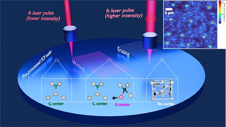
An artistic depiction of a new method to create high-quality color-centers (qubits) in silicon at specific locations using ultrafast laser pulses (femtosecond, or one quadrillionth of a second). The inset at the top-right shows an experimentally observed optical signal (photoluminescence) from the qubits, with their structures displayed at the bottom. (Credit: Kaushalya Jhuria/Berkeley Lab)
See the science paper for further instructive material with images.
The researchers learned that processing silicon with a low femtosecond laser intensity in the presence of hydrogen helped to create the Ci color centers. Further experiments showed that increasing the laser intensity can increase the mobility of hydrogen, which passivates undesirable color centers without damaging the silicon lattice, Schenkel explained.
A theoretical analysis performed by Liang Tan, staff scientist in Berkeley Lab’s Molecular Foundry [below], shows that the brightness of the Ci color center is boosted by several orders of magnitude in the presence of hydrogen, confirming their observations from laboratory experiments.
“The femtosecond laser pulses can kick out hydrogen atoms or bring them back, allowing the programmable formation of desired optical qubits in precise locations,” Jhuria said.
The team plans to use the technique to integrate optical qubits in quantum devices such as reflective cavities and waveguides, and to discover new spin photon qubit candidates with properties optimized for selected applications.
“Now that we can reliably make color centers, we want to get different qubits to talk to each other – which is an embodiment of quantum entanglement – and see which ones perform the best. This is just the beginning,” said Jhuria.
“The ability to form qubits at programmable locations in a material like silicon that is available at scale is an exciting step towards practical quantum networking and computing,” said Cameron Geddes, Director of the ATAP Division.
Theoretical analysis for the study was performed at the Department of Energy’s National Energy Research Scientific Computing Center (NERSC) at Berkeley Lab with support from the NERSC QIS@Perlmutter program.
The Molecular Foundry and NERSC are DOE Office of Science user facilities at Berkeley Lab.
This work was supported by the DOE Office of Fusion Energy Sciences.
See the full article here .
Comments are invited and will be appreciated, especially if the reader finds any errors which I can correct.

five-ways-keep-your-child-safe-school-shootings
Please help promote STEM in your local schools.
![]()

Bringing Science Solutions to the World
In the world of science, The Lawrence Berkeley National Laboratory (Berkeley Lab) is synonymous with “excellence.” A number of Nobel prizes are associated with Berkeley Lab. Lab scientists are members of the The National Academy of Sciences, one of the highest honors for a scientist in the United States. A number of our scientists have won the National Medal of Science, our nation’s highest award for lifetime achievement in fields of scientific research. A number of our engineers have been elected to the The National Academy of Engineering, and a number of our scientists have been elected into The Institute of Medicine. In addition, Berkeley Lab has trained thousands of university science and engineering students who are advancing technological innovations across the nation and around the world.
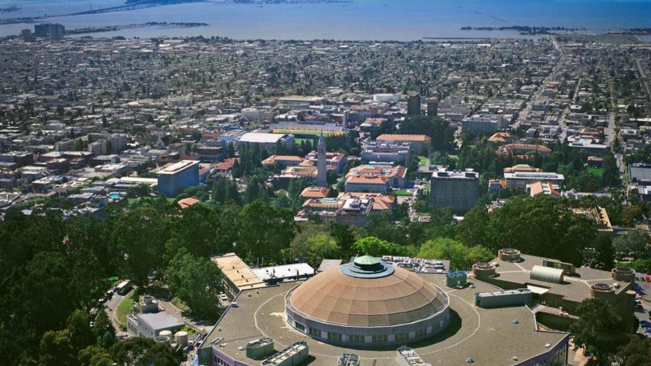
Berkeley Lab is a member of the national laboratory system supported by The DOE through its Office of Science. It is managed by the University of California-Berkeley and is charged with conducting unclassified research across a wide range of scientific disciplines. Located on a 202-acre site in the hills above The University of California-Berkeley campus that offers spectacular views of the San Francisco Bay, Berkeley Lab employs a large number of scientists, engineers and support staff. Technologies developed at Berkeley Lab have generated billions of dollars in revenues, and thousands of jobs. Savings as a result of Berkeley Lab developments in lighting and windows, and other energy-efficient technologies, have also been in the billions of dollars.
Berkeley Lab was founded in 1931 by Ernest Orlando Lawrence, a University of California-Berkeley physicist who won the 1939 Nobel Prize in physics for his invention of the cyclotron, a circular particle accelerator that opened the door to high-energy physics. It was Lawrence’s belief that scientific research is best done through teams of individuals with different fields of expertise, working together. His teamwork concept is a Berkeley Lab legacy that continues today.
History
1931–1941
The laboratory was founded on August 26, 1931, by Ernest Lawrence, as the Radiation Laboratory of the University of California-Berkeley, associated with the Physics Department. It centered physics research around his new instrument, the cyclotron, a type of particle accelerator for which he was awarded the Nobel Prize in Physics in 1939.

LBNL 88 inch cyclotron.

Throughout the 1930s, Lawrence pushed to create larger and larger machines for physics research, courting private philanthropists for funding. He was the first to develop a large team to build big projects to make discoveries in basic research. Eventually these machines grew too large to be held on the university grounds, and in 1940 the lab moved to its current site atop the hill above campus. Part of the team put together during this period includes two other young scientists who went on to establish large laboratories; J. Robert Oppenheimer founded The DOE’s Los Alamos Laboratory, and Robert Wilson founded The DOE’s Fermi National Accelerator Laboratory.
1942–1950
Leslie Groves visited Lawrence’s Radiation Laboratory in late 1942 as he was organizing the Manhattan Project, meeting J. Robert Oppenheimer for the first time. Oppenheimer was tasked with organizing the nuclear bomb development effort and founded today’s DOE Los Alamos National Laboratory to help keep the work secret. At the RadLab, Lawrence and his colleagues developed the technique of electromagnetic enrichment of uranium using their experience with cyclotrons. The “calutrons” (named after the University) became the basic unit of the massive Y-12 facility in Oak Ridge, Tennessee. Lawrence’s lab helped contribute to what have been judged to be the three most valuable technology developments of the war (the atomic bomb, proximity fuse, and radar). The cyclotron, whose construction was stalled during the war, was finished in November 1946. The Manhattan Project shut down two months later.
1951–2018
After the war, the Radiation Laboratory became one of the first laboratories to be incorporated into the Atomic Energy Commission (AEC) (now The Department of Energy . The most highly classified work remained at Los Alamos, but the RadLab remained involved. Edward Teller suggested setting up a second lab similar to Los Alamos to compete with their designs. This led to the creation of an offshoot of the RadLab (now The DOE’s Lawrence Livermore National Laboratory) in 1952. Some of the RadLab’s work was transferred to the new lab, but some classified research continued at Berkeley Lab until the 1970s, when it became a laboratory dedicated only to unclassified scientific research.
Shortly after the death of Lawrence in August 1958, the UC Radiation Laboratory (both branches) was renamed the Lawrence Radiation Laboratory. The Berkeley location became the Lawrence Berkeley Laboratory in 1971, although many continued to call it the RadLab. Gradually, another shortened form came into common usage, LBNL. Its formal name was amended to Ernest Orlando Lawrence Berkeley National Laboratory in 1995, when “National” was added to the names of all DOE labs. “Ernest Orlando” was later dropped to shorten the name. Today, the lab is commonly referred to as “Berkeley Lab”.
The Alvarez Physics Memos are a set of informal working papers of the large group of physicists, engineers, computer programmers, and technicians led by Luis W. Alvarez from the early 1950s until his death in 1988. Over 1700 memos are available on-line, hosted by the Laboratory.
The lab remains owned by the Department of Energy , with management from the University of California-Berkeley. Companies such as Intel were funding the lab’s research into computing chips.
Science mission
From the 1950s through the present, Berkeley Lab has maintained its status as a major international center for physics research, and has also diversified its research program into almost every realm of scientific investigation. Its mission is to solve the most pressing and profound scientific problems facing humanity, conduct basic research for a secure energy future, understand living systems to improve the environment, health, and energy supply, understand matter and energy in the universe, build and safely operate leading scientific facilities for the nation, and train the next generation of scientists and engineers.
The Laboratory’s 20 scientific divisions are organized within six areas of research: Computing Sciences; Physical Sciences; Earth and Environmental Sciences; Biosciences; Energy Sciences; and Energy Technologies. Berkeley Lab has six main science thrusts: advancing integrated fundamental energy science; integrative biological and environmental system science; advanced computing for science impact; discovering the fundamental properties of matter and energy; accelerators for the future; and developing energy technology innovations for a sustainable future. It was Lawrence’s belief that scientific research is best done through teams of individuals with different fields of expertise, working together. His teamwork concept is a Berkeley Lab tradition that continues today.
Berkeley Lab operates five major National User Facilities for the DOE Office of Science:
The Advanced Light Source (ALS) is a synchrotron light source with 41 beam lines providing ultraviolet, soft x-ray, and hard x-ray light to scientific experiments.

The ALS is one of the world’s brightest sources of soft x-rays, which are used to characterize the electronic structure of matter and to reveal microscopic structures with elemental and chemical specificity. About 2,500 scientist-users carry out research at ALS every year. Berkeley Lab is proposing an upgrade of ALS which would increase the coherent flux of soft x-rays by two-three orders of magnitude.
Berkeley Lab Laser Accelerator (BELLA) Center


The DOE Joint Genome Institute supports genomic research in support of the DOE missions in alternative energy, global carbon cycling, and environmental management. The JGI’s partner laboratories are Berkeley Lab, the DOE’s Lawrence Livermore National Laboratory, the DOE’s Oak Ridge National Laboratory (ORNL), the DOE’s Pacific Northwest National Laboratory (PNNL), and the DOE’s HudsonAlpha Institute for Biotechnology . The JGI’s central role is the development of a diversity of large-scale experimental and computational capabilities to link sequence to biological insights relevant to energy and environmental research. A large number of scientist-users take advantage of JGI’s capabilities for their research every year.
The LBNL Molecular Foundry is a multidisciplinary nanoscience research facility. Its seven research facilities focus on Imaging and Manipulation of Nanostructures; Nanofabrication; Theory of Nanostructured Materials; Inorganic Nanostructures; Biological Nanostructures; Organic and Macromolecular Synthesis; and Electron Microscopy. Approximately 700 scientist-users make use of these facilities in their research every year.
The DOE’s NERSC National Energy Research Scientific Computing Center is the scientific computing facility that provides large-scale computing for the DOE’s unclassified research programs. Its current systems provide over 3 billion computational hours annually. NERSC supports 6,000 scientific users from universities, national laboratories, and industry.
DOE’s NERSC National Energy Research Scientific Computing Center at Lawrence Berkeley National Laboratory.
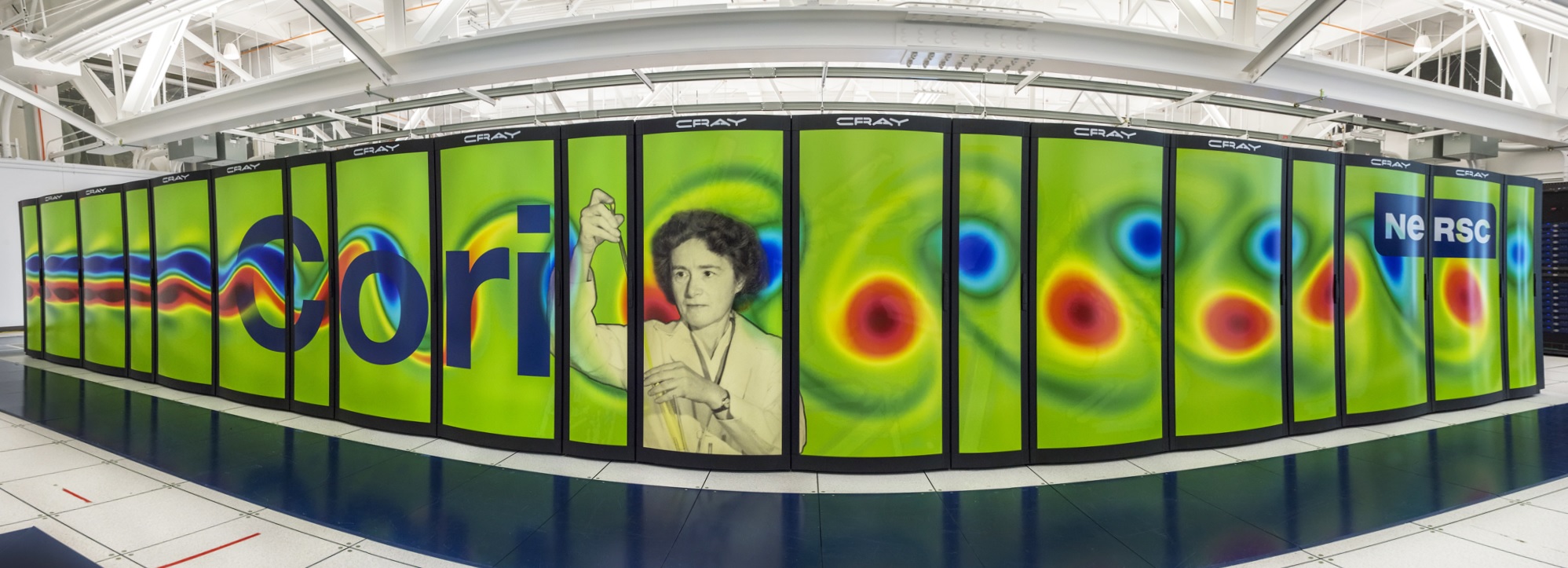
NERSC is a DOE Office of Science User Facility.


The DOE’s Energy Science Network is a high-speed network infrastructure optimized for very large scientific data flows. ESNet provides connectivity for all major DOE sites and facilities, and the network transports roughly 35 petabytes of traffic each month.
Berkeley Lab is the lead partner in the DOE’s Joint Bioenergy Institute (JBEI), located in Emeryville, California. Other partners are the DOE’s Sandia National Laboratory, the University of California (UC) campuses of Berkeley and Davis, the Carnegie Institution for Science , and the DOE’s Lawrence Livermore National Laboratory (LLNL). JBEI’s primary scientific mission is to advance the development of the next generation of biofuels – liquid fuels derived from the solar energy stored in plant biomass. JBEI is one of three new U.S. Department of Energy (DOE) Bioenergy Research Centers (BRCs).
Berkeley Lab has a major role in two DOE Energy Innovation Hubs. The mission of the Joint Center for Artificial Photosynthesis (JCAP) is to find a cost-effective method to produce fuels using only sunlight, water, and carbon dioxide. The lead institution for JCAP is the California Institute of Technology and Berkeley Lab is the second institutional center. The mission of the Joint Center for Energy Storage Research (JCESR) is to create next-generation battery technologies that will transform transportation and the electricity grid. The DOE’s Argonne National Laboratory leads JCESR and Berkeley Lab is a major partner.
